TNY256YN Power Integrations, TNY256YN Datasheet - Page 5
TNY256YN
Manufacturer Part Number
TNY256YN
Description
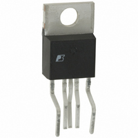
IC OFFLINE SWIT UVLO HV TO220
Manufacturer
Power Integrations
Series
TinySwitch® Plusr
Datasheet
1.TNY256YN.pdf
(20 pages)
Specifications of TNY256YN
Output Isolation
Isolated
Frequency Range
115 ~ 140kHz
Voltage - Output
700V
Power (watts)
11W
Operating Temperature
-40°C ~ 150°C
Package / Case
TO-220-7 (Formed Leads), 5 Leads
Output Voltage
5.8 V
Input / Supply Voltage (max)
265 VAC
Input / Supply Voltage (min)
85 VAC
Duty Cycle (max)
69 %
Switching Frequency
130 KHz
Supply Current
255 uA
Operating Temperature Range
- 40 C to + 150 C
Mounting Style
Through Hole
Lead Free Status / RoHS Status
Lead free / RoHS Compliant
Other names
596-1218-5
TNY256YN
TNY256YN
Available stocks
Company
Part Number
Manufacturer
Quantity
Price
Company:

Part Number:
TNY256YN
Manufacturer:
POWER
Quantity:
15 000
Part Number:
TNY256YN
Manufacturer:
POWER
Quantity:
20 000


Figure 8. TNY256 Power-up With External Resistor (2 M )
power level at the lowest input voltage, the calculated inductance
will ramp up the current to the current limit before the DC
limit is reached.
Enable Function
TNY256 senses the EN/UV pin to determine whether or not to
proceed with the next switch cycle as described earlier. Once
a cycle is started, it always completes the cycle (even when the
EN/UV pin changes state half way through the cycle). This
operation results in a power supply whose output voltage ripple
is determined by the output capacitor, amount of energy per
switch cycle and the delay of the feedback.
The EN/UV pin signal is generated on the secondary by
comparing the power supply output voltage with a reference
voltage. The EN/UV pin signal is high when the power supply
output voltage is less than the reference voltage.
In a typical implementation, the EN/UV pin is driven by an
optocoupler. The collector of the optocoupler transistor is
connected to the EN/UV pin and the emitter is connected to the
SOURCE pin. The optocoupler LED is connected in series with
a Zener across the DC output voltage to be regulated. When the
output voltage exceeds the target regulation voltage level
(optocoupler diode voltage drop plus Zener voltage), the
optocoupler diode will start to conduct, pulling the EN/UV pin
low. The Zener can be replaced by a TL431 device for
improved accuracy.
The EN/UV pin pull-down current threshold is nominally
50 A, but is set to 40 A the instant the threshold is exceeded.
This is reset back to 50 A when the EN/UV pull-down current
drops below the current threshold of 40 A.
200
100
400
200
10
0
5
0
0
0
V
V
V
Connected to EN/UV Pin.
DC-BUS
BYPASS
DRAIN
Time (ms)
1
MAX
2
Figure 9. TNY256 Power-up Without External Resistor Connected
ON/OFF Control
The internal clock of the TNY256 runs all the time. At the
beginning of each clock cycle, it samples the EN/UV pin to
decide whether or not to implement a switch cycle. If the
EN/UV pin is high (< 40 A), then a switching cycle takes
place. If the EN/UV pin is low (greater than 50 A) then no
switching cycle occurs, and the EN/UV pin status is sampled
again at the start of the subsequent clock cycle.
At full load, TNY256 will conduct during the majority of its
clock cycles (Figure6). At loads less than full load, it will
“skip” more cycles in order to maintain voltage regulation at the
secondary output. At light load or no load, almost all cycles will
be skipped (Figure7). A small percentage of cycles will
conduct to support the power consumption of the power supply.
The response time of the TNY256 ON/OFF control scheme is
very fast compared to normal PWM control. This provides tight
regulation and excellent transient response.
Power Up/Down
The TNY256 requires only a 0.1 F capacitor on the BYPASS
pin. Because of the small size of this capacitor, the power-up
delay is kept to an absolute minimum, typically 0.3 ms. Due to
the fast nature of the ON/OFF feedback, there is no overshoot
at the power supply output. When an external resistor (2 M )
is connected to the EN/UV pin, the power MOSFET switching
will be delayed during power-up until the DC line voltage
exceeds the threshold (100 V). Figures 8 and 9 illustrate the
power-up timing waveform of TNY256 in applications with
and without an external resistor (2 M ) connected to the
EN/UV pin.
200
100
400
200
10
0
5
0
0
0
V
V
V
to EN/UV Pin.
DC-BUS
BYPASS
DRAIN
Time (ms)
1
TNY256
7/01
C
5
2
Related parts for TNY256YN
Image
Part Number
Description
Manufacturer
Datasheet
Request
R

Part Number:
Description:
Energy Efficient, Low Power Off-line Switcher
Manufacturer:
Power Integrations, Inc.
Datasheet:

Part Number:
Description:
SOP-16
Manufacturer:
Power Integrations
Datasheet:
Part Number:
Description:
DIP8
Manufacturer:
Power Integrations
Datasheet:
Part Number:
Description:
TO-263
Manufacturer:
Power Integrations
Datasheet:
Part Number:
Description:
TO-263
Manufacturer:
Power Integrations
Datasheet: