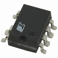
LNK520GN Power Integrations, LNK520GN Datasheet - Page 6

LNK520GN
Manufacturer Part Number
LNK520GN
Description
IC SWIT OCP CV/CC HV 8SMD
Manufacturer
Power Integrations
Series
LinkSwitch®r
Datasheet
1.LNK520PN.pdf
(20 pages)
Specifications of LNK520GN
Output Isolation
Isolated
Frequency Range
24 ~ 49.5kHz
Voltage - Output
700V
Power (watts)
5.50W
Operating Temperature
-40°C ~ 150°C
Package / Case
8-SMD Gull Wing, 7 Leads
Output Voltage
5.6 V
Input / Supply Voltage (max)
265 VAC
Input / Supply Voltage (min)
85 VAC
Duty Cycle (max)
80 %
Switching Frequency
42 KHz
Supply Current
0.75 mA
Operating Temperature Range
- 40 C to + 150 C
Mounting Style
SMD/SMT
For Use With
596-1006 - KIT DESIGN ACCELERATOR ADAPTER
Lead Free Status / RoHS Status
Lead free / RoHS Compliant
Available stocks
Company
Part Number
Manufacturer
Quantity
Price
Company:
Part Number:
LNK520GN
Manufacturer:
POWER
Quantity:
15 000
Part Number:
LNK520GN
Manufacturer:
POWER
Quantity:
20 000
Company:
Part Number:
LNK520GN-TL
Manufacturer:
ST
Quantity:
245
Company:
Part Number:
LNK520GN-TL
Manufacturer:
PowerInt
Quantity:
3 000
Part Number:
LNK520GN-TL
Manufacturer:
POWER
Quantity:
20 000
To achieve this goal, the minimum voltage feedback threshold
should be set at V
CC to CV transition point of the inherent characteristic will
always occur below the voltage feedback threshold. However, the
output voltage tolerance is then increased, since the inherent CV
characteristic tolerance below V
of the optocoupler feedback circuit.
The LNK520 can also be used in the high-side configuration as
shown in Figure 9(a). This configuration provides a very low
component count solution with an approximate CV/CC power
supply output characteristic. A typical output characteristic
envelope is shown in Figure 9(b).
This configuration is ideal for very low cost charger and adapter
applications where output CC tolerance is loose or unspecified.
Typical applications include low cost chargers and adapters
where direct replacement for a linear transformer is required.
In applications with a high voltage DC input voltage, the circuit
is further simplified with the removal of input rectifiers, EMI
filter choke and input capacitors. Typical applications of this
type include auxiliary supplies in domestic appliances and
industrial applications.
In the high-side configuration, the CONTROL pin receives
feedback current through R1 generated by the voltage across
C2. To a first order, this voltage is proportional to V
V
the off time of the LNK520 switching cycle. The output CV
regulation is therefore determined by how well the voltage across
C2 tracks the output voltage. This tracking is influenced by the
value of the transformer leakage inductance, which introduces
an error. This error, which is partially filtered by R2 and C2,
causes a slope in the output CV regulation characteristic.
The LNK520 is optimized for use with a bias winding where
tracking of feedback voltage and output voltage is typically
better than it is in the high-side configuration of Figure 9 (a).
As a consequence, the increased leakage error in the high-side
configuration causes the output current to increase with falling
output voltage, as indicated by the output CC characteristic
envelope in Figure 9 (b).
Figure 9. High-side Configuration Using LNK520: (a) Schematic Outline; (b) Typical Output Characteristic Envelope.
OUT
6
is reflected to the primary and appears across C2 during
LNK520
E
2/05
V
IN
O(MAX)
. This will ensure that the voltage at the
O(MAX)
LinkSwitch
D
(a)
is added to the tolerance
C
R1
R2
D1
C1
S
C2
LNK520
OUT
since
C4
D2
V
OUT
In this high-side configuration, the SOURCE pins and circuit
board traces form a switching node. Extra care should be taken
to optimize EMI performance. The LNK520 internal MOSFET
switching characteristics have been designed to significantly
reduce EMI, particularly in the radiated spectrum (>30 MHz).
However, the SOURCE trace area should be minimized and
EMI filter components should be distanced from the SOURCE
node whenever possible. In embedded applications where a
high voltage DC input voltage is available, system level EMI
filtering is typically located away from the power supply and
circuit board layout is less critical.
Applications Example
The circuit shown in Figure 10 shows a typical implementation
of an approximate constant voltage / constant current (CV/CC)
charger using LinkSwitch in the low-side configuration. This
design delivers 2.75 W with nominal peak power point voltage
of 5.5 V and a current of 500 mA (Figure 11). Efficiency is
greater than 65% over an input range of 85 VAC to 265 VAC.
The bridge rectifier, D1-D4, rectifies the AC input. The rectified
AC is smoothed by C1 and C2, with inductor L1 forming a pi-filter
to filter differential mode conducted EMI. Resistor RF1 is a
fusible, flameproof type providing protection from primary-side
short circuits and line surges and provides additional differential
EMI filtering. The switching frequency of 42 kHz allows such
a simple EMI filter to be used without the need for a Y capacitor
while still meeting international EMI standards.
When power is applied, high voltage DC appears at the DRAIN
pin of LinkSwitch (U1). The CONTROL pin capacitor C5 is
then charged through a switched high voltage current source
connected internally between the DRAIN and CONTROL
pins. When the CONTROL pin reaches approximately
5.6 V relative to the SOURCE pin, the internal current source
is turned off. The internal control circuitry is activated and the
high voltage MOSFET starts to switch, using the energy in C5
to power the IC.
V
OUT
(b)
Typical
Characteristic
PI-3854-031804
I
OUT


