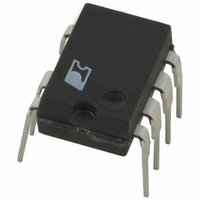
TNY266PN Power Integrations, TNY266PN Datasheet

TNY266PN
Specifications of TNY266PN
Available stocks
Related parts for TNY266PN
TNY266PN Summary of contents
Page 1
TNY263-268 TinySwitch-II Family Enhanced, Energy Efficient, Low Power Off-line Switcher Product Highlights TinySwitch-II Features Reduce System Cost • Fully integrated auto-restart for short circuit and open loop fault protection – saves external component costs • Built-in circuitry practically eliminates audible ...
Page 2
TNY263-268 BYPASS (BP) LINE UNDER-VOLTAGE 240 µA 50 µA ENABLE JITTER 1 OSCILLATOR ENABLE/ UNDER- VOLTAGE (EN/UV) Figure 2. Functional Block Diagram. Pin Functional Description DRAIN (D) Pin: Power MOSFET drain connection. Provides internal operating current ...
Page 3
TinySwitch-II Functional Description TinySwitch-II combines a high voltage power MOSFET switch with a power supply controller in one device. Unlike conventional PWM (pulse width modulator) controllers, TinySwitch-II uses a simple ON/OFF control to regulate the output voltage. The TinySwitch-II controller ...
Page 4
TNY263-268 70 °C (typical) is provided to prevent overheating of the PC board due to a continuous fault condition. Current Limit The current limit circuit senses the current in the power MOSFET. When this current exceeds the internal threshold (I ...
Page 5
SOURCE pin. The optocoupler LED is connected in series with a Zener diode across the DC output voltage to be regulated. When the output voltage exceeds the target regulation voltage level (optocoupler LED voltage drop plus Zener voltage), the ...
Page 6
TNY263-268 V EN CLOCK D MAX I DRAIN V DRAIN Figure 9. TinySwitch-II Operation at Very Light Load. During power-down, when an external resistor is used, the power MOSFET will switch for 50 ms after the output loses regulation. The ...
Page 7
D1 1N4005 D2 1N4005 C1 3.3 µF 85-265 400 V VAC RF1 8.2 Ω Fusible R1 1.2 kΩ 1N4005 1N4005 L1 2.2 mH Figure 14. 2.5 W Constant Voltage, Constant Current Battery Charger with Universal Input (85-265 VAC). ...
Page 8
TNY263-268 2.5 W CV/CC Cell-Phone Charger As an example, Figure 14 shows a TNY264 based 5 V, 0.5 A, cellular phone charger operating over a universal input range (85 VAC to 265 VAC). The inductor (L1) forms a π-filter in ...
Page 9
PERFORMANCE SUMMARY Continuous Output Power: 10.24 W ≥ 75% Efficiency: 140-375 VDC INPUT C1 0.01 µ TNY266P +12 VDC µ Figure 15 Standby Supply. PERFORMANCE ...
Page 10
TNY263-268 Key Application Considerations TinySwitch-II vs. TinySwitch Table 2 compares the features and performance differences between the TNY254 device of the TinySwitch family with the TinySwitch-II family of devices. Many of the new features eliminate the need for or reduce ...
Page 11
A secondary output with a Schottky rectifier diode. 3. Assumed efficiency of 77% (TNY267 & TNY268), 75% (TNY265 & TNY266) and 73% (TNY263 & TNY264). 4. The parts are board mounted with SOURCE pins soldered to ...
Page 12
... TNY263-268 Input Filter Capacitor + HV — TOP VIEW C BP Figure 17. Recommended Circuit Board Layout for TinySwitch-II with Under-Voltage Lock Out Resistor. PC Board Cleaning Power Integrations does not recommend the use of “no clean” flux 4/05 Safety Spacing Y1- Capacitor PRI TinySwitch-II Opto- coupler ...
Page 13
DRAIN Voltage .................................. ................ -0 700 V DRAIN Peak Current: TNY263......................................400 mA TNY264......................................400 mA TNY265......................................440 mA TNY266......................................560 mA TNY267......................................720 mA TNY268......................................880 mA EN/UV Voltage ................................................ -0 EN/UV Current .................................................... 100 mA BYPASS Voltage .................................................. ...
Page 14
TNY263-268 Parameter Symbol CONTROL FUNCTIONS (cont.) BYPASS Pin V Voltage BP BYPASS Pin V Voltage Hysteresis BPH EN/UV Pin Line Under-Voltage I LUV Threshold CIRCUIT PROTECTION Current Limit I LIMIT Initial Current Limit I INIT Leading Edge t Blanking Time ...
Page 15
Parameter Symbol OUTPUT ON-State R Resistance DS(ON) OFF-State Drain I Leakage Current DSS Breakdown BV Voltage DSS Rise Time t R Fall Time t F Drain Supply Voltage Output EN/UV t Delay EN/UV Output Disable t Setup Time DST Auto-Restart ...
Page 16
TNY263-268 NOTES: A. Total current consumption is the sum of I switching) and the sum of I and Since the output MOSFET is switching difficult to isolate the switching current from the supply current at ...
Page 17
D EN/ NOTE: This test circuit is not applicable for current limit or output characteristic measurements. Figure 18. TinySwitch-II General Test Circuit. Figure 19. TinySwitch-II Duty Cycle Measurement. 470 Ω 470 Ω S1 ...
Page 18
TNY263-268 Typical Performance Characteristics 1.1 1.0 0.9 -50 - 100 125 150 Junction Temperature (°C) Figure 22. Breakdown vs. Temperature. 1.2 1 TNY263 0.8 TNY264-266 TNY267 TNY268 0.6 0.4 0 Temperature (°C) ...
Page 19
Typical Performance Characteristics (cont.) 1000 100 Scaling Factors: TNY263 TNY264 TNY265 TNY266 10 TNY267 TNY268 1 0 100 200 300 Drain Voltage (V) Figure 28. C vs. Drain Voltage. OSS 1.0 1.0 1.5 15 2.0 3.5 ...
Page 20
TNY263-268 PART ORDERING INFORMATION TNY 264 ⊕ .004 (.10) -E- .240 (6.10) .260 (6.60) Pin 1 .367 (9.32) -D- .387 (9.83) .125 (3.18) .145 (3.68) -T- SEATING PLANE .100 (2.54) BSC .048 (1.22) .053 ...
Page 21
D S .004 (.10) -E- .240 (6.10) .260 (6.60) Pin 1 .100 (2.54) (BSC) .367 (9.32) -D- .387 (9.83) .125 (3.18) .145 (3.68) .032 (.81) .048 (1.22) .037 (.94) .053 (1.35) SMD-8B .137 (3.48) MINIMUM .372 (9.45) .388 (9.86) ...
Page 22
TNY263-268 22 G 4/05 ...
Page 23
Revision Notes Corrected first page spacing and sentence in description describing innovative design. 2) Corrected Frequency Jitter in Figure 4 and Frequency Jitter in Parameter Table. 3) Added last sentence to Over Temperature Protection section. 4) ...
Page 24
... For the latest updates, visit our website: www.powerint.com Power Integrations reserves the right to make changes to its products at any time to improve reliability or manufacturability. Power Integrations does not assume any liability arising from the use of any device or circuit described herein. POWER INTEGRATIONS MAKES NO WARRANTY HEREIN AND SPECIFICALLY DISCLAIMS ALL WARRANTIES INCLUDING, WITHOUT LIMITATION, THE IMPLIED WARRANTIES OF MERCHANTABILITY, FITNESS FOR A PARTICULAR PURPOSE, AND NON-INFRINGEMENT OF THIRD PARTY RIGHTS ...


