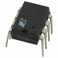
TNY253P Power Integrations, TNY253P Datasheet - Page 5

TNY253P
Manufacturer Part Number
TNY253P
Description
IC OFFLINE SWIT OTP OCP HV 8DIP
Manufacturer
Power Integrations
Series
TinySwitch®r
Datasheet
1.TNY253GN-TL.pdf
(20 pages)
Specifications of TNY253P
Output Isolation
Isolated
Frequency Range
40 ~ 48kHz
Voltage - Output
700V
Power (watts)
2W
Operating Temperature
-40°C ~ 150°C
Package / Case
8-DIP (0.300", 7.62mm)
Output Voltage
5.8 V
Input / Supply Voltage (max)
265 VAC
Input / Supply Voltage (min)
85 VAC
Duty Cycle (max)
68 %
Switching Frequency
44 KHz
Supply Current
140 uA
Operating Temperature Range
- 40 C to + 150 C
Mounting Style
Through Hole
Lead Free Status / RoHS Status
Contains lead / RoHS non-compliant
Available stocks
Company
Part Number
Manufacturer
Quantity
Price
Company:
Part Number:
TNY253P
Manufacturer:
POWER
Quantity:
5 510
Company:
Part Number:
TNY253P
Manufacturer:
MOTOROLA
Quantity:
5 510
Company:
Part Number:
TNY253PN
Manufacturer:
FREESCALE
Quantity:
652
Part Number:
TNY253PN
Manufacturer:
POWER
Quantity:
20 000
Figure 6. TinySwitch Operation at Light Load.
130 kHz Switching Frequency (TNY255)
The switching frequency (with no cycle skipping) is set at
130 kHz. This allows the TNY255 to deliver 10 W while still
using the same size, low cost transformer (EE16) as used by the
TNY253/254 for lower power applications.
BYPASS Pin Capacitor
The BYPASS pin uses a small 0.1 µF ceramic capacitor for
decoupling the internal power supply of the TinySwitch.
Application Examples
Television Standby
TinySwitch is an ideal solution for low cost, high efficiency
standby power supplies used in consumer electronic products
such as TVs. Figure 9 shows a 7.5 V, 1.3 W flyback circuit that
uses TNY253 for implementing a TV standby supply. The
circuit operates from the DC high voltage already available
from the main power supply. This input voltage can range from
120 to 375 VDC depending on the input AC voltage range that
the TV is rated for. Capacitor C1 filters the high voltage DC
supply, and is necessary only if there is a long trace length from
the source of the DC supply to the inputs of the TV standby
circuit. The high voltage DC bus is applied to the series
combination of the primary winding of T1 and the integrated
high voltage MOSFET inside the TNY253. The low operating
frequency of the TNY253 (44 kHz), allows a low cost snubber
circuit C2 and R1 to be used in place of a primary clamp circuit.
In addition to limiting the DRAIN turn off voltage spike to a
safe value, the RC snubber also reduces radiated video noise by
DC
V
I
CLOCK
DRAIN
DRAIN
MAX
V
EN
PI-2261-061198
V
V
Figure 7. TinySwitch Power-Up Timing Diagram.
DRAIN
DRAIN
lowering the dv/dt of the DRAIN waveform, which is critical for
video applications such as TV and VCR. On fixed frequency
PWM and RCC circuits, use of a snubber will result in an
undesirable fixed AC switching loss that is independent of load.
The ON/OFF control on the TinySwitch eliminates this problem
by scaling the effective switching frequency and therefore,
switching loss linearly with load. Thus the efficiency of the
supply stays relatively constant down to a fraction of a watt of
output loading.
The secondary winding is rectified and filtered by D1 and C4 to
create the 7.5 V output. L1 and C5 provide additional filtering.
The output voltage is determined by the sum of the optocoupler
U2 LED forward drop (~ 1 V) and Zener diode VR1 voltage.
The resistor R2, maintains a bias current through the Zener to
improve its voltage tolerance.
Figure 8. TinySwitch Power Down Timing Diagram.
V
V
IN
IN
0
0
100
.2
200
.4
Time (ms)
Time (ms)
300
.6
TNY253/254/255
12 V
12 V
400
.8
4/03
D
500
1
5
0 V
0 V
0 V
0 V


