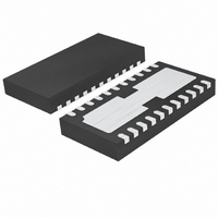
LTC4090EDJC#PBF Linear Technology, LTC4090EDJC#PBF Datasheet - Page 25

LTC4090EDJC#PBF
Manufacturer Part Number
LTC4090EDJC#PBF
Description
IC USB POWER MANAGER 22-DFN
Manufacturer
Linear Technology
Datasheet
1.LTC4090EDJCPBF.pdf
(28 pages)
Specifications of LTC4090EDJC#PBF
Function
Power Management
Battery Type
Lithium-Ion (Li-Ion), Lithium-Polymer (Li-Pol)
Voltage - Supply
4.35 V ~ 5.5 V
Operating Temperature
-40°C ~ 85°C
Mounting Type
Surface Mount
Package / Case
22-WFDFN Exposed Pad
Supply Voltage Range
4.35V To 5.5V
Operating Temperature Range
-40°C To +85°C
Digital Ic Case Style
DFN
No. Of Pins
22
Msl
MSL 1 - Unlimited
Termination Type
SMD
Supply Voltage Min
4.35V
Rohs Compliant
Yes
Filter Terminals
SMD
Frequency
2.7MHz
Lead Free Status / RoHS Status
Lead free / RoHS Compliant
Available stocks
Company
Part Number
Manufacturer
Quantity
Price
APPLICATIONS INFORMATION
be estimated by calculating the regulator power loss from
an effi ciency measurement, and subtracting the catch
diode loss.
The difference between this equation and that for the
LTC4090 is the last term, which represents the power
dissipation in the battery charger. For a typical application,
an example of this calculation would be:
Like the LTC4090 example, this examples assumes 87%
effi ciency, V
600mA resulting in about 2W total power dissipation.
It is important to solder the exposed backside of the pack-
age to a ground plane. This ground should be tied to other
copper layers below with thermal vias; these layers will
spread the heat dissipated by the LTC4090/LTC4090-5.
Additional vias should be placed near the catch diode.
Adding more copper to the top and bottom layers and
WITH C3 GND PAD
AND SEPERATED
P
P
VIAS CONNECTED TO ALL
(
(
SIDE-BY-SIDE
I
1A + 0.6A
D
D
GND PLANES WITHOUT
BAT
C1 AND D1
GND PADS
= 1– 0.87
= 1– η
SOLDERED TO PCB.
(
U1 THERMAL PAD
(
THERMAL RELIEF
+I
OUT
HVIN
)
Figure 10. Suggested Board Layout
)
+ 5V – 3.7V
)
• 5V • I
)
(
+ 5V – V
(
• 5V • 1A + 0.6A
= 12V, V
(
(
(
(
BAT
BAT
BAT
)
• 1A = 1.97W
+I
= 3.7V, I
)
OUT
•I
BAT
)
)
MINIMIZE TRACE LENGTH
)
)
– 0.4V • 1–
– V
BAT
D
= 1A and I
• 1–
⎛
⎝ ⎜
⎛
⎝ ⎜
MINIMIZE D1, L1,
C3, U1, SW PIN LOOP
12V
V
5V
5V
HVIN
4090 F10
⎞
⎠ ⎟
OUT
•
⎞
⎠ ⎟
•
=
tying this copper to the internal planes with vias can
reduce thermal resistance further. With these steps, the
thermal resistance from die (i.e., junction) to ambient can
be reduced to θ
Board Layout Considerations
As discussed in the previous section, it is critical that
the exposed metal pad on the backside of the LTC4090/
LTC4090-5 package be soldered to the PC board ground.
Furthermore, proper operation and minimum EMI requires
a careful printed circuit board (PCB) layout. Note that large,
switched currents fl ow in the power switch (between the
HVIN and SW pins), the catch diode and the HVIN input
capacitor. These components, along with the inductor and
output capacitor, should be placed on the same side of
the circuit board, and their connections should be made
on that layer. Place a local, unbroken ground plane below
these components. The loop formed by these components
should be as small as possible.
Additionally, the SW and BOOST nodes should be kept
as small as possible. Figure 10 shows the recommended
component placement with trace and via locations.
High frequency currents, such as the high voltage input
current of the LTC4090/LTC4090-5, tend to fi nd their way
along the ground plane on a mirror path directly beneath
the incident path on the top of the board. If there are slits
or cuts in the ground plane due to other traces on that layer,
the current will be forced to go around the slits. If high
frequency currents are not allowed to fl ow back through
their natural least-area path, excessive voltage will build
up and radiated emissions will occur. See Figure 11.
Figure 11. Ground Currents Follow Their Incident
Path at High Speed. Slices in the Ground Plane
Cause High Voltage and Increased Emissions.
JA
LTC4090/LTC4090-5
= 40°C/W.
4090 F11
25
4090fc


