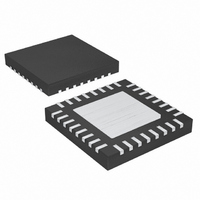
DS2726G+ Maxim Integrated Products, DS2726G+ Datasheet - Page 12

DS2726G+
Manufacturer Part Number
DS2726G+
Description
IC PROT LI+ 5-10CELL 32-TQFP
Manufacturer
Maxim Integrated Products
Datasheet
1.DS2726G.pdf
(16 pages)
Specifications of DS2726G+
Function
Over/Under Voltage Protection
Battery Type
Lithium-Ion (Li-Ion)
Voltage - Supply
5 V ~ 50 V
Operating Temperature
-20°C ~ 85°C
Mounting Type
Surface Mount
Package / Case
32-TQFN Exposed Pad
Lead Free Status / RoHS Status
Lead free / RoHS Compliant
The DS2726 allows the OV threshold to be set using the
overvoltage select pins. The OV threshold is configured
using the OVS0 and OVS1 pins according to Table 3.
For cell balancing to begin the DS2726 must detect a
charger. The charge-balancing configuration pin
(CBCFG) controls how the IC detects a charger. If
CBCFG is pulled to GND, balancing is enabled when
the charge-current comparator detects a charger. This
detection occurs when V
is pulled to V
SLEEP pin is driven to a logic-high state. Note that cell
balancing must be enabled and a valid cell-balancing
voltage must exist for cell balancing to occur.
The DS2726 allows the cell-balancing threshold to be set
using the cell-balance select pins. The threshold is config-
ured using the CBS0 and CBS1 pins according to Table 4.
Setting the cell-balancing voltage threshold to zero dis-
ables the cell-balancing circuitry. The nominal cell-bal-
5-Cell to 10-Cell Li+ Protector with
Cell Balancing
Table 3. OV Threshold Configuration
Table 4. Cell-Balancing Threshold Configuration
12
______________________________________________________________________________________
Configuration of Cell-Balancing
OVS0
OVS1
CBS0
CBS1
PIN
PIN
Configuration of Overvoltage
CC
, cell balancing is enabled when the
Enabling Cell Balancing
4.10
0.00
V
V
V
V
PKP
IL
IL
IL
IL
Voltage Threshold
> V
VIN
4.15
0.05
V
V
V
V
IM
IM
IL
IL
+ V
CELL-BALANCING VOLTAGE THRESHOLD (OFFSET FROM V
Threshold
CDET
4.20
0.10
. If CBCFG
V
V
V
V
IH
IH
IL
IL
NOMINAL OV THRESHOLD (V)
4.25
0.15
V
V
V
V
IM
IM
IL
IL
ancing voltage is never allowed a value below 3.75V.
Setting the OVS0 and OVS1 pins low while the CBS0
and CBS1 pins are high results in a cell-balancing volt-
age (V
Nominal Cell-Balancing Voltage:
Balancing begins when any cell’s voltage is greater
than V
cell balancing is enabled, the corresponding internal
FET (from V
the charge current around the cell. The external resis-
tors on V00–V10 should be chosen to limit the balanc-
ing current to a maximum of 200mA. This prevents
damaging the internal cell-balancing FETs.
The DS2726 has three distinct states during balancing.
A voltage measurement state of 5/32 t
is followed by a balancing state where even numbered
cells are balanced for 123/32 t
Another voltage measurement state of 5/32 t
periods then occurs. This is followed by a balancing
state where odd numbered cells are balanced for
123/32 t
ancing current of approximately half the maximum bal-
ance current. Cell balancing terminates when all cell
voltages are greater than V
Sequence section.
V
BAL
4.30
0.20
V
V
V
V
BAL
BAL
IM
IM
IM
IM
OCD
= V
) of 3.75V.
. When the balancing condition is met and
x
OV
time periods. This gives an average bal-
to V
4.35
0.25
– Cell-Balancing Voltage Threshold
V
V
V
V
IM
x-1
IH
IH
IM
) is enabled, shunting a portion of
4.40
0.30
V
V
V
V
BAL
IH
IH
IL
IL
. See the Measurement
OV
) (V)
OCD
4.45
0.35
OCD
V
V
V
V
IM
IH
IM
IH
time periods.
time periods
OCD
4.50
0.40
V
V
V
V
IH
IH
IH
IH
time


