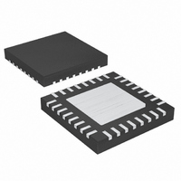
DS2726G+ Maxim Integrated Products, DS2726G+ Datasheet - Page 9

DS2726G+
Manufacturer Part Number
DS2726G+
Description
IC PROT LI+ 5-10CELL 32-TQFP
Manufacturer
Maxim Integrated Products
Datasheet
1.DS2726G.pdf
(16 pages)
Specifications of DS2726G+
Function
Over/Under Voltage Protection
Battery Type
Lithium-Ion (Li-Ion)
Voltage - Supply
5 V ~ 50 V
Operating Temperature
-20°C ~ 85°C
Mounting Type
Surface Mount
Package / Case
32-TQFN Exposed Pad
Lead Free Status / RoHS Status
Lead free / RoHS Compliant
The DS2726 provides the protection features for a
5-cell to 10-cell Li+ battery pack. The Li+ protection cir-
cuit allows for pin-configured selection of OV threshold
and the cell-balancing threshold. DOC and SC thresh-
olds and delays are component programmable.
Sleep Mode is a low-power state where the FETs are
open and the IC is not monitoring voltages. During
Wake Mode, the IC measures voltages and drives the
FETs to the appropriate state.
Upon initial connection to cells, the DS2726 enters
Sleep Mode. The IC also enters Sleep Mode if a UV
condition is detected. Sleep Mode can be initiated any
time by pulling the SLEEP pin low while a charger-
detect condition does not exist. During Sleep Mode
there is a pulldown current from PKP to GND.
V
exit wake from Sleep Mode.
When a charger is detected and V
tion, the part measures all cells for undervoltage and
Table 1. Li+ Protection Conditions and DS2726 Responses
*All voltages are with respect to GND. CC Off: V
Note 13: The DC FET remains off until V
Note 14: With test current I
Note 15: If a DOC condition persists indefinitely and a UV condition is reached, the IC does not enter Sleep Mode.
Overvoltage (OV)
Undervoltage (UV)
(Note 15)
Discharge Overcurrent
(DOC) (Note 15)
Short Circuit (SC)
PKP
must be within V
CONDITION*
_______________________________________________________________________________________
Detailed Description
TP
TST
of V
flowing from V
V
VIN
THRESHOLD
V
V
V
SNS
SNS
CELL
CELL
5-Cell to 10-Cell Li+ Protector with
(V
< V
CELL
< V
PKP
CC
> V
< V
Sleep Mode
RDOC
RSC
achieves regula-
OV
UV
IN
> V
> V
to PKP.
CC
UV_REL
VIN
= V
- V
PKP
.
ACTIVATION
TP
, DC Off: V
) to
DELAY
t
t
DOCD
t
t
OVD
UVD
SCD
DC
overvoltage. Then the IC begins controlling the CC and
DC FETs as shown in Table 1. Care should be taken to
ensure that the SLEEP pin is not held low during a wake
condition.
The DS2726 has two different methods for detecting a
charger connection. The methods are pin programma-
ble at the CBCFG pin. If CBCFG is pulled to GND, then
charge detection occurs when V
CBCFG is pulled to V
when the SLEEP pin is driven to a logic-high state.
In Active Mode, the DS2726 constantly monitors V00–
V10 to protect the battery from overvoltage and under-
voltage. The voltage on the SNS pin is monitored and
compared to the voltages on RDOC and RSC to protect
against excessive discharge currents (discharge over-
current and short circuit). Table 1 summarizes the con-
ditions that activate the protection circuit, the response
of the DS2726, and the thresholds that release it from a
protection state.
= V
VIN
.
CC Off, DC Off,
RESPONSE
Sleep Mode
CC Off
DC Off
DC Off
Li+ Protection Circuitry
Cell Balancing
CC
, then charge detection occurs
V
PKP
V
V
RELEASE THRESHOLD
PKP
PKP
V
V
Charger Detect
CELL
> V
CELL
CBCFG > V
PKP
CBCFG < V
CBCFG < V
V
V
SLEEP > V
> V
> V
PKP
PKP
VIN
V
CELL
< V
> V
VIN
VIN
> V
> V
> V
+ V
UV_REL
UV_REL
- V
- V
VIN
< V
VIN
VIN
CDET
TP
TP
IH
IH
IL
IL
CE
- V
- V
+ V
(Note 14)
(Note 15)
and
and
and
then
, then
, then
(Note 13)
TP
TP
CDET
. If
9


