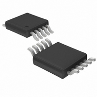
LTC4050EMS-4.1#TR Linear Technology, LTC4050EMS-4.1#TR Datasheet - Page 5

LTC4050EMS-4.1#TR
Manufacturer Part Number
LTC4050EMS-4.1#TR
Description
IC BATT CHRG CNTRL LI-ION 10MSOP
Manufacturer
Linear Technology
Datasheet
1.LTC4050EMS-4.1.pdf
(12 pages)
Specifications of LTC4050EMS-4.1#TR
Function
Charge Management
Battery Type
Lithium-Ion (Li-Ion)
Voltage - Supply
4.5 V ~ 10 V
Operating Temperature
-40°C ~ 85°C
Mounting Type
Surface Mount
Package / Case
10-TFSOP, 10-MSOP (0.118", 3.00mm Width)
Lead Free Status / RoHS Status
Contains lead / RoHS non-compliant
Other names
LTC4050EMS-4.1TR
LTC4050EMS4.1TR
LTC4050EMS4.1TR
Available stocks
Company
Part Number
Manufacturer
Quantity
Price
PIN
BAT (Pin 1): Battery Sense Input. A precision internal
resistor divider on this pin sets the final float voltage. The
resistor divider is disconnected in sleep mode to reduce
the current drain on the battery. A bypass capacitor of
10 F or more is required to keep the loop stable when the
battery is not connected.
NTC (Pin 2): Thermistor Interface Input. A 10k
Curve 2 NTC thermistor (or other 10k NTC thermistor
with a room temperature beta of around 3400) is con-
nected from this pin to ground. The charge cycle will be
disabled and the timer will be placed on hold if the
thermistor temperature is above 50 C or below 0 C.
CHRG (Pin 3): Charge Status Open-Drain Output. When
the battery is charging, the CHRG pin is pulled low by an
internal N-channel MOSFET. When the charge current
drops to 10% of the full-scale current for more than 15ms,
the N-channel MOSFET turns off and a 32 A current
source is connected from the CHRG pin to GND. When the
timer runs out or the input supply is removed, the current
source is disconnected and the CHRG pin becomes high
impedance.
TIMER (Pin 4): Timer Capacitor and Constant-Voltage
Mode Disable Input Pin. The timer period is set by placing
a capacitor, C
(C
GND will disable the internal timer function and the C/10
function.
GND (Pin 5): Ground.
TIMER
U
FUNCTIONS
• 3 hours)/(0.1 F). Shorting the TIMER pin to
U
TIMER
, to GND. The timer period is t
U
TIMER
Dale
=
PROG (Pin 6): Charge Current Program and Shutdown
Input Pin. The charge current is programmed by connect-
ing a resistor, R
= (V
into shutdown by floating the PROG pin and allowing the
internal 2.3 A current source to pull the pin above the 3.6V
shutdown threshold voltage.
DRV (Pin 7): Drive Output Pin for the P-Channel MOSFET
or PNP Transistor. The impedance is high at this pin,
therefore, if a PNP pass transistor is used, it must have
high gain.
V
from 4.5V to 10V. Bypass this pin with a 1 F capacitor.
When V
into sleep mode, dropping I
SENSE (Pin 9): Current Sense Input. A sense resistor,
R
Select a resistor value that will develop approximately
100mV at the programmed full-scale charge current.
This resistor is chosen using the following equation:
ACPR (Pin 10): Wall Adapter Present Output. When the
input voltage (wall adaptor) is applied to the LTC4050, this
pin is pulled to ground by an internal N-channel MOSFET
that is capable of sinking 5mA suitable for driving an
external LED.
CC
SENSE
R
PROG
(Pin 8): Positive Input Supply Voltage. V
SENSE
, must be connected from V
BAT
• 800 )/(R
= (V
is within 54mV of V
PROG
PROG
• 800 )/(R
PROG
to ground. The charge current is I
• R
CC
SENSE
to 5 A.
CC
PROG
, the LTC4050 is forced
). The IC can be forced
CC
• I
to the SENSE pin.
BAT
LTC4050
)
CC
can range
5
BAT
4050f


