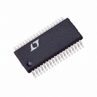
LTC1759CG Linear Technology, LTC1759CG Datasheet - Page 7

LTC1759CG
Manufacturer Part Number
LTC1759CG
Description
IC SMART BATTERY CHARGER 36SSOP
Manufacturer
Linear Technology
Datasheet
1.LTC1759CGPBF.pdf
(28 pages)
Specifications of LTC1759CG
Function
Charge Management
Battery Type
Smart Batteries
Voltage - Supply
11 V ~ 24 V
Operating Temperature
0°C ~ 70°C
Mounting Type
Surface Mount
Package / Case
36-SSOP (0.200", 5.30mm Width)
Lead Free Status / RoHS Status
Contains lead / RoHS non-compliant
Available stocks
Company
Part Number
Manufacturer
Quantity
Price
Company:
Part Number:
LTC1759CG
Manufacturer:
LT
Quantity:
4 071
Part Number:
LTC1759CG
Manufacturer:
LINEAR/凌特
Quantity:
20 000
Part Number:
LTC1759CG#PBF
Manufacturer:
LINEAR/凌特
Quantity:
20 000
Part Number:
LTC1759CG#TR
Manufacturer:
LT/凌特
Quantity:
20 000
Part Number:
LTC1759CG#TRPBF
Manufacturer:
LTNEAR
Quantity:
20 000
PIN
Input Power-Related Pins
UV (Pin 7): Charger Section Undervoltage Lockout Pin.
The rising threshold is 6.7V with a hysteresis of 0.5V.
Switching stops in undervoltage lockout. Connect this
input to the input voltage source with no resistor divider.
UV must be pulled below 0.7V when there is no input
voltage source (5k resistor from adapter output to ground
is required) to obtain the lowest quiescent battery current.
INFET (Pin 8): Gate Drive to Input P-channel FET. For very
low dropout applications, use an external P-channel FET to
connect the adapter output and V
7.8V below V
CLP (Pin 9): Positive Input to the Input Current Limit
Amplifier CL1. When used to limit supply current, a filter
(R3 and C1 of Figure 10) is needed to filter out the
switching noise. The threshold is set at 92mV.
CLN (Pin 10): Negative Input to the Input Current Limit
Amplifier CL1. It should be connected to V
bypass capacitor C2 for less noise).
COMP1 (Pin 11): Compensation Node for the Input Cur-
rent Limit Amplifier CL1. At input adapter current limit, this
node rises to 1V. By forcing COMP1 low with an external
transistor, amplifier CL1 will be defeated (no adapter
current limit). COMP1 can source 200 A. Ground (to
AGND) this pin if the adapter current limiting function is
not used.
Battery Charging-Related Pins
BOOST (Pin 1): This pin is used to bootstrap and supply
power for the topside power switch gate drive and control
circuity. In normal operation, V
internally generated 8.6V regulator V
+ 9.1V when TGATE is high. Do not force an external
voltage on BOOST pin.
TGATE (Pin 2): This pin provides gate drive to the topside
power FET. When TGATE is driven on, the gate voltage will
be approximately equal to V
5 to 10 should be used from this pin to the gate of the
topside FET.
U
FUNCTIONS
U
CC
.
U
SW
+ 6.6V. A series resistor of
BOOST
CC
. INFET is clamped to
GBIAS
is powered from an
, V
CC
BOOST
(to the V
V
CC
CC
SW (Pin 3): This pin is the reference point for the floating
topside gate drive circuitry. It is the common connection
for the top and bottom side switches and the output
inductor. This pin switches between ground and V
very high dv/dt rates. Care needs to be taken in the PC
layout to keep this node from coupling to other sensitive
nodes. A 1A Schottky clamping diode should be placed
very close to the chip from the ground pin to this pin to
prevent the chip substrate diode from turning on. See
Applications Information for more details.
SYNC (Pin 4): External Clock Synchronization Input. Pulse
width range: 10% to 90%.
SDB (Shutdown Bar) (Pin 5): Active Low Digital Input. The
charger is disabled when asserted. This pin is connected
to the CHGEN pin to enable charger control through the
SMBus interface.
CHGEN (Pin 12): Digital Output to Enable Charger Func-
tion. Connect CHGEN to SDB.
I
external resistor, R
current programming input, the PROG pin of the battery
charger section, which sets the range of the charging
current.
I
this pin and DGND. The value of the external resistor
programs the range and resolution of the programmed
charger current. See Electrical Characteristics table for
more information.
V
this pin and DGND. The value of the external resistor
programs the range and resolution of the V
Electrical Characteristics table for more information.
V
resistor divider, which provides battery voltage feedback
to the charger.
SET
LIMIT
LIMIT
SET
(Pin 17): Open-Drain CMOS Switch to DGND. An
(Pin 26): This is the tap point of the programmable
(Pin 24): An external resistor is connected between
(Pin 25): An external resistor is connected between
SET
, is connected from I
SET
LTC1759
divider. See
SET
CC
to the
with
7


