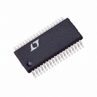
LTC1759CG#TRPBF Linear Technology, LTC1759CG#TRPBF Datasheet - Page 8

LTC1759CG#TRPBF
Manufacturer Part Number
LTC1759CG#TRPBF
Description
IC SMART BATTERY CHARGER 36SSOP
Manufacturer
Linear Technology
Datasheet
1.LTC1759CGPBF.pdf
(28 pages)
Specifications of LTC1759CG#TRPBF
Function
Charge Management
Battery Type
Smart Batteries
Voltage - Supply
11 V ~ 24 V
Operating Temperature
0°C ~ 70°C
Mounting Type
Surface Mount
Package / Case
36-SSOP (0.200", 5.30mm Width)
Lead Free Status / RoHS Status
Lead free / RoHS Compliant
Available stocks
Company
Part Number
Manufacturer
Quantity
Price
PIN
LTC1759
V
the current mode PWM. Switching starts at 0.9V. Higher
V
operation. A capacitor of at least 0.33 F to AGND filters out
noise and controls the rate of soft start.
PROG (Pin 28): This pin is for programming the charging
current and for system loop compensation. During normal
operation, the pin voltage is approximately 2.465V.
SENSE (Pin 29): Current Amplifier CA1 Input. Sensing
must be at the positive terminal of the battery.
SPIN (Pin 30): This pin is for the internal amplifier
CA1 bias. It must be connected to R
Figure 1.
BAT1 (Pin 31): Current Amplifier CA1 Input.
BOOSTC (Pin 33): This pin is used to bootstrap and supply
the current sense amplifier CA1 for very low dropout
conditions. V
battery voltage. A diode and a capacitor are needed to get
the voltage from V
V
floating or tied to V
lower than V
BGATE (Pin 35): Drives the gate of the bottom external
N-channel FET of the charger buck converter.
Monitor/Fault Diagnostic Pins
DCDIV (Pin 21): Supply Divider Input. This is a high
impedance comparator input with a 1V threshold (rising
edge) and hysteresis.
DCIN (Pin 22): Input connected to the DC input source to
monitor the DC input for power-fail condition.
BAT2 (Pin 23): Sensing Point for Voltage Control Loop.
Connect this to the positive terminal of the battery.
8
C
C
CC
U
(Pin 27): This is the control signal of the inner loop of
corresponds to higher charging current in normal
is always 3V or greater than V
FUNCTIONS
U
CC
CC
.
can be as low as only 0.4V above the
BOOST
CC
U
. Do not force this pin to a voltage
. If low dropout is not needed and
BAT
, this pin can be left
SENSE
as shown in
Internal Power Supply Pins
AGND (Pin 6): DC Accurate Ground for Analog Circuitry.
V
this pin with 0.1 F.
DGND (Pin 18): Ground for Digital Circuitry and DACs.
Should be connected to AGND at the negative terminal
of the charger output filter capacitor.
V
Bypass this pin with 0.47 F.
GBIAS (Pin 34): 8.6V Regulator Output for Bootstrapping
V
needed. Switching will stop if V
PGND (Pin 36): High Current Ground Return for Charger
Gate Drivers.
SBS Interface Pins
INTB (Interrupt Bar) (Pin 13): Active Low Interrupt Output
to Host. Signals host that there has been a change of status
in the charger registers and that the host should read the
LTC1759 status registers to determine if any action on its
part is required. This signal can be connected to the
optional SMBALERT# line of the SMBus. Open drain with
weak current source pull-up to V
it to be pulled to 5V externally, see Figure 2).
SDA (Pin 14): SMBus Data Signal from Main (Host-
controlled) SMBus.
SCL (Pin 15): SMBus Clock Signal from Main (Host-
Controlled) SMBus. External pull-up resistor is required.
THERM (Pin 19): Thermistor Force/Sense Pin to Smart
Battery. See Electrical Characteristics table for more
detail. Maximum allowed combined capacitance on THERM
and RNR is 75pF.
RNR (Pin 20): Thermistor Force/Sense Pin to Smart
Battery. See Electrical Characteristics table for more
detail. Maximum allowed combined capacitance on THERM
and RNR is 75pF.
DD
CC
BOOST
(Pin 32): Power Input for Battery Charger Section.
(Pin 16): Low Voltage Power Supply Input. Bypass
and V
BOOSTC
. A bypass capacitor of at least 2 F is
DD
BOOST
(with Schottky to allow
drops below 7.1V.


