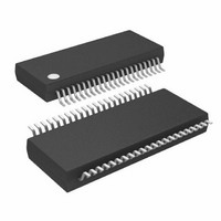
LTC6802IG-1#TRPBF Linear Technology, LTC6802IG-1#TRPBF Datasheet - Page 11

LTC6802IG-1#TRPBF
Manufacturer Part Number
LTC6802IG-1#TRPBF
Description
IC MONITOR BATT STACK MC 44-SSOP
Manufacturer
Linear Technology
Datasheet
1.LTC6802IG-1PBF.pdf
(38 pages)
Specifications of LTC6802IG-1#TRPBF
Function
Battery Monitor
Battery Type
Lithium-Ion (Li-Ion)
Voltage - Supply
4 V ~ 50 V
Operating Temperature
-40°C ~ 85°C
Mounting Type
Surface Mount
Package / Case
44-SOP (0.200", 5.30mm Width)
Lead Free Status / RoHS Status
Lead free / RoHS Compliant
Available stocks
Company
Part Number
Manufacturer
Quantity
Price
TIMING DIAGRAM
OPERATION
THEORY OF OPERATION
The LTC6802-1 is a data acquisition IC capable of mea-
suring the voltage of 12 series connected battery cells.
An input multiplexer connects the batteries to a 12-bit
delta-sigma analog to digital converter (ADC). An internal
10ppm voltage reference combined with the ADC give the
LTC6802-1 its outstanding measurement accuracy. The
inherent benefits of the delta-sigma ADC versus other types
of ADCs (e.g. successive approximation) are explained
in Advantages of Delta-Sigma ADCs in the Applications
Information section.
Communication between the LTC6802-1 and a host pro-
cessor is handled by a SPI compatible serial interface. As
shown in Figure 1, the LTC6802-1’s can pass data up and
down a stack of devices using simple diodes for isolation.
This operation is described in Serial Port in the Applica-
tions Information section.
The LTC6802-1 also contains circuitry to balance cell volt-
ages. Internal MOSFETs can be used to discharge cells.
These internal MOSFETs can also be used to control external
balancing circuits. Figure 1 illustrates cell balancing by
SCKI
CSBI
SDO
SDI
PREVIOUS COMMAND
D4
t
1
D3
D3
t
2
t
8
Timing Diagram of the Serial Interface
D2
t
D2
4
t
3
D1
internal discharge. Figure 4 shows the S pin controlling
an external balancing circuit. It is important to note that
the LTC6802-1 makes no decisions about turning on/off
the internal MOSFETs. This is completely controlled by
the host processor. The host processor writes values to
a configuration register inside the LTC6802-1 to control
the switches. The watchdog timer on the LTC6802-1 will
turn off the discharge switches if communication with the
host processor is interrupted.
OPEN CONNECTION DETECTION
When a cell input (C pin) is open, it affects two cell mea-
surements. Figure 2 shows an open connection to C3,
in an application without external filtering between the C
pins and the cells. During normal ADC conversions (that
is, using the STCVAD command), the LTC6802 will give
near zero readings for B3 and B4 when C3 is open. The
zero reading for B3 occurs because during the measure-
ment of B3, the ADC input resistance will pull C3 to the
C2 potential. Similarly, during the measurement of B4, the
ADC input resistance pulls C3 to the C4 potential.
D1
t
D0
6
D0
t
5
CURRENT COMMAND
t
7
D7 … D4
D7 … D4
LTC6802-1
D3
68021 TD
D3
11
68021fa


