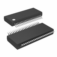
LTC6802IG-1#TRPBF Linear Technology, LTC6802IG-1#TRPBF Datasheet - Page 20

LTC6802IG-1#TRPBF
Manufacturer Part Number
LTC6802IG-1#TRPBF
Description
IC MONITOR BATT STACK MC 44-SSOP
Manufacturer
Linear Technology
Datasheet
1.LTC6802IG-1PBF.pdf
(38 pages)
Specifications of LTC6802IG-1#TRPBF
Function
Battery Monitor
Battery Type
Lithium-Ion (Li-Ion)
Voltage - Supply
4 V ~ 50 V
Operating Temperature
-40°C ~ 85°C
Mounting Type
Surface Mount
Package / Case
44-SOP (0.200", 5.30mm Width)
Lead Free Status / RoHS Status
Lead free / RoHS Compliant
Available stocks
Company
Part Number
Manufacturer
Quantity
Price
LTC6802-1
APPLICATIONS INFORMATION
The voltage mode pin (V
side serial port is configured as voltage mode or current
mode. For the bottom device in a daisy-chain stack, this
pin must be pulled high (tied to V
in the daisy chain must have this pin pulled low (tied to V
to designate current mode communication. To designate
the top-of-stack device for polling commands, the TOS
pin on the top device of a daisy chain must be tied high.
The other devices in the stack must have TOS tied low.
See Figure 1.
Data Link Layer
Clock Phase And Polarity: The LTC6802-1 SPI-compat-
ible interface is configured to operate in a system using
CPHA=1 and CPOL=1. Consequently, data on SDI must
be stable during the rising edge of SCKI.
20
CSBI
SCKI
CSBI
SCKI
SDO
SDI
SDI
MODE
MSB (CMD)
MSB (CMD)
) determines whether the low
REG
BIT6 (CMD)
BIT6 (CMD)
). The other devices
Figure 8. Transmission Format (Write)
Figure 9. Transmission Format (Read)
– )
LSB (CMD)
LSB (CMD)
Data Transfers: Every byte consists of 8 bits. Bytes are
transferred with the most significant bit (MSB) first. On a
write, the data value on SDI is latched into the device on
the rising edge of SCKI (Figure 8). Similarly, on a read,
the data value output on SDO is valid during the rising
edge of SCKI and transitions on the falling edge of SCKI
(Figure 9).
CSBI must remain low for the entire duration of a com-
mand sequence, including between a command byte and
subsequent data. On a write command, data is latched in
on the rising edge of CSBI.
After a polling command has been entered, the SDO output
will immediately be driven by the polling state, with the
SCKI input ignored (Figure 10). See the Toggle Polling
and Level Polling sections.
MSB (DATA)
MSB (DATA)
LSB (DATA)
LSB (DATA)
68021 F09
68021 F08
68021fa


