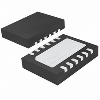
LTC4265IDE#PBF Linear Technology, LTC4265IDE#PBF Datasheet - Page 14

LTC4265IDE#PBF
Manufacturer Part Number
LTC4265IDE#PBF
Description
IC CTRLR PD INTERFACE HP 12-DFN
Manufacturer
Linear Technology
Type
Power over Ethernet Switch (PoE)r
Datasheet
1.LTC4265IDEPBF.pdf
(20 pages)
Specifications of LTC4265IDE#PBF
Applications
Remote Peripherals (Industrial Controls, Cameras, Data Access)
Internal Switch(s)
Yes
Operating Temperature
-40°C ~ 85°C
Mounting Type
Surface Mount
Package / Case
12-WFDFN Exposed Pad
Input Voltage
60V
Supply Current
1.35mA
Digital Ic Case Style
DFN
No. Of Pins
12
Uvlo
30V
Operating Temperature Range
-40°C To +85°C
Msl
MSL 1 - Unlimited
Termination Type
SMD
Rohs Compliant
Yes
Filter Terminals
SMD
Controller Type
Hot Swap
Lead Free Status / RoHS Status
Lead free / RoHS Compliant
Available stocks
Company
Part Number
Manufacturer
Quantity
Price
APPLICATIONS INFORMATION
LTC4265
Input Capacitor
The IEEE 802.3af/at standard includes an impedance
requirement in order to implement the AC disconnect
function. A 0.1μF capacitor (C14 in Figure 7) is used to
meet this AC impedance requirement.
Transient Voltage Suppressor
The LTC4265 specifi es an absolute maximum voltage of
100V and is designed to tolerate brief overvoltage events.
However, the pins that interface to the outside world can
routinely see excessive peak voltages. To protect the
LTC4265, install a transient voltage suppressor (D3) be-
tween the input diode bridge and the LTC4265 as shown
in Figure 7.
Classifi cation Resistor (R
The R
corresponding to the PD power classifi cation. Select the
value of R
between the R
or fl oat the R
not required. The resistor tolerance must be 1% or better
to avoid degrading the overall accuracy of the classifi ca-
tion circuit.
Load Capacitor
The IEEE 802.3af/at specifi cation requires that the PD
maintains a minimum load capacitance of 5μF and does
not specify a maximum load capacitor. However, if the
load capacitor is too large, there may be a problem with
inadvertent power shutdown by the PSE.
14
CLASS
CLASS
resistor sets the classifi cation load current,
CLASS
CLASS
from Table 2 and connect the resistor
pin if the classifi cation load current is
and V
CLASS
IN
pins as shown in Figure 4,
)
This occurs when the PSE voltage drops quickly. The input
diode bridge reverses bias, and the PD load momentarily
powers off the load capacitor. If the PD does not draw
power within the PSE’s 300ms disconnection delay, the
PSE may remove power from the PD. Thus, it is necessary
to evaluate the load current and capacitance to ensure that
an inadvertent shutdown cannot occur.
The load capacitor can store signifi cant energy when fully
charged. The PD design must ensure that this energy is
not inadvertently dissipated in the LTC4265. For example,
if the GND pin shorts to V
current will fl ow through the parasitic body diode of the
internal MOSFET and may cause permanent damage to
the LTC4265.
Power Good Interface
The LTC4265 provides complementary power good sig-
nals to simplify the DC/DC converter interface. Using the
power good signal to delay converter operation until the
load capacitor is fully charged is highly recommended to
ensure trouble free start up.
Figure 8 presents examples of power good interface cir-
cuits. The active high PWRGD pin has an open collector
transistor referenced to VOUT while the active low PWRGD
pin has a high voltage, open-drain MOSFET referenced
to V
the DC/DC converter. When using PWRGD, diode D9 and
resistor R
excessive reverse voltage.
IN
. The designer can choose either signal to enable
S
protects the converter shutdown pin from
IN
while the capacitor is charged,
4265fa


