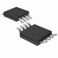
LTC4211CMS8 Linear Technology, LTC4211CMS8 Datasheet - Page 30

LTC4211CMS8
Manufacturer Part Number
LTC4211CMS8
Description
IC CONTROLLER HOT SWAP 8-MSOP
Manufacturer
Linear Technology
Type
Hot-Swap Controllerr
Datasheet
1.LTC4211IMS8PBF.pdf
(36 pages)
Specifications of LTC4211CMS8
Applications
General Purpose
Internal Switch(s)
No
Voltage - Supply
2.5 V ~ 16.5 V
Operating Temperature
0°C ~ 70°C
Mounting Type
Surface Mount
Package / Case
8-TSSOP, 8-MSOP (0.118", 3.00mm Width)
Lead Free Status / RoHS Status
Contains lead / RoHS non-compliant
Available stocks
Company
Part Number
Manufacturer
Quantity
Price
Company:
Part Number:
LTC4211CMS8
Manufacturer:
LT
Quantity:
10 000
Part Number:
LTC4211CMS8
Manufacturer:
LT/凌特
Quantity:
20 000
Part Number:
LTC4211CMS8#2KMPBF
Manufacturer:
LT/凌特
Quantity:
20 000
Part Number:
LTC4211CMS8#PBF
Manufacturer:
LINEAR/凌特
Quantity:
20 000
APPLICATIO S I FOR ATIO
SUPPLY OVERVOLTAGE DETECTION/
PROTECTION USING FILTER PIN
In addition to using external protection devices around the
LTC4211 for large scale transient protection, low power
Zener diodes can be used with the LTC4211’s FILTER pin
to act as a supply overvoltage detection/protection circuit
on either the high side (input) or low side (output) of the
external pass transistor. Recall that internal control cir-
cuitry keeps the LTC4211 GATE voltage from ramping up
if V
(V
High Side (Input) Overvoltage Protection
As shown in Figure 23, a low power Zener diode can be
used to sense an overvoltage condition on the input
(high) side of the main 5V supply. In this example, a low
bias current 1N4691 Zener diode is chosen to protect the
system. Here, the Zener diode is connected from V
the LTC4211’s FILTER pin (Pin 3 MS). If the input voltage
to the system is greater than 6.8V during start-up, the
voltage on the FILTER pin is pulled higher than its 1.156V
LTC4211
30
FILTER
FILTER
ON/OFF
FAULT
RESET
GND
5V
> 1.236V) causes FAULT to be asserted low.
> 1.156V, or when an external fault condition
CONNECTOR
BACKPLANE
(FEMALE)
U
CONNECTOR
PCB EDGE
(MALE)
U
Figure 23. LTC4211MS High Side Overvoltage Protection Implementation
LONG
SHORT
SHORT
SHORT
LONG
W
R4
10k
10k
R6
Z1*
R5
10k
R7
10k
U
R3
10Ω
6.2V
C1
0.1µF
Z2
C
47pF
CC
FILTER
to
threshold. As a result, the GATE pin is not allowed to ramp
and the second timing cycle will not commence until the
supply overvoltage condition is removed. Should the
supply overvoltage condition occur during normal op-
eration, internal control logic would trip the electronic
circuit breaker and the GATE would be pulled to ground,
shutting OFF the external pass transistor. If a lower
supply overvoltage threshold is desired, use a Zener
diode with a smaller breakdown voltage.
A timing diagram for illustrating LTC4211 operation under
a high side overvoltage condition is shown in Figure 24.
The start-up sequence in this case (between Time Points
1 and 2) is identical to any other start-up sequence under
normal operating conditions. At Time Point 2A, the input
supply voltage causes the Zener diode to conduct thereby
forcing V
asserted low and the TIMER pin voltage ramps down. At
Time Point 4, the LTC4211 checks if V
C
10nF
TIMER
1
2
3
4
5
RESET
ON
FILTER
TIMER
GND
FILTER
LTC4211
SENSE
FAULT
GATE
Z1 = 1SMA10A OR SMAJ10A
Z2 = 1N4691
* OPTIONAL
V
FB
CC
> 1.156V. At Time Point 3, FAULT is
10
9
8
7
6
0.007Ω
R
SENSE
Si4410DY
Q1
4211 F23
FILTER
R1
36k
R2
15k
+
< 1.156V.
C
LOAD
V
5V
5A
OUT
4211fa


