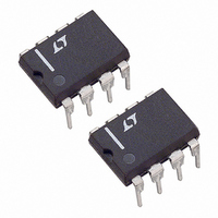
LTC1422CN8#PBF Linear Technology, LTC1422CN8#PBF Datasheet - Page 11

LTC1422CN8#PBF
Manufacturer Part Number
LTC1422CN8#PBF
Description
IC CONTROLLER HOT SWAP 8-DIP
Manufacturer
Linear Technology
Type
Hot-Swap Controllerr
Datasheet
1.LTC1422CS8PBF.pdf
(16 pages)
Specifications of LTC1422CN8#PBF
Applications
General Purpose
Internal Switch(s)
No
Voltage - Supply
2.7 V ~ 12 V
Operating Temperature
0°C ~ 70°C
Mounting Type
Through Hole
Package / Case
8-DIP (0.300", 7.62mm)
Lead Free Status / RoHS Status
Lead free / RoHS Compliant
APPLICATIONS
Since the pass transistor is in a common source configu-
ration, care must be taken to limit the inrush current into
capacitor C3. One way is to precharge C3 using resistor
R4. As the input supply is ramping up, current is flowing
through R4 and charging the capacitor C3. Once the input
supply crosses 38V, there is a timing cycle followed by the
ramp-up of the GATE pin. By this time the capacitor C3 is
sufficiently charged, thereby limiting the inrush current.
Another method to limit the inrush current is to slow down
the ramp-up rate of the GATE pin.
Hot Swapping 48V DC/DC Module with
Active High On/Off Control Signal
This application is identical to the previous except for the
polarity of the module’s on/off signal. The polarity reversal
is accomplished by transistor Q3 in Figure 13.
Hot Swapping Redundant 48V
In critical situations, redundant input supplies are neces-
sary. In Figure 14 a redundant 48V input is switched to a
power module. Supplies 1 and 2 are wire OR’ed using two
diodes D2 and D3. This results in the most negative of
these two supplies being used to drive the power module.
If one of the supplies is disconnected or a fuse opens, the
fault signal will be activated via diodes D4 and D5 and the
reset comparator at the FB pin. The GATE IN signal on the
Vicor module is controlled using the high voltage PNP Q2.
Once the module’s minus input pin is more negative than
the base of Q2 plus a diode drop, Q2 will turn off and the
module will turn on. This occurs when the source of Q1
U
INFORMATION
U
V
5V
IN
CURRENT LIMIT: 2.5A
1
2
3
4
RESET
ON
TIMER
GND
LTC1422
W
SENSE
GATE
V
FB
CC
Figure 11. Switching 5V and Generating 3.3V
8
7
6
5
0.02
5%
R1
U
MMFT2N02ELT1
Q1
R3
10
5%
C2
0.1 F
16V
1.6M
5%
MMFT2N02ELT1
R6
plus a Zener voltage (D1) is more positive than the drain
of Q1 (in other words, when the switching FET Q1 has only
7.5V across its drain source).
Hot Swapping 48V Module with Isolated Controller
A power supervisory controller will sometimes reside on
an isolated supply with responsibility for other supplies.
Figure 15 shows how to Hot Swap a controller’s 5V supply
and a 48V module using two LTC1422s. Assuming the 5V
supply comes up first, the controller waits for a power
good signal from the 48V circuit. Once it receives the right
signals the controller activates the GATE IN pin of the Vicor
power module.
Power Supply Sequencer
A circuit that forces two supply voltages to power up
together is shown in Figure 16. The input supply voltages
may power up in any sequence, but both input voltages
must be within tolerance before Q1 and Q2 turn on. Back-
to-back transistors Q1 and Q2 ensure isolation between
the two supplies.
When the 5V input powers up before 3.3V, Q1 and Q2
remain off and the 5V output remains off until the 3.3V
input is within tolerance as sensed by resistors R1 and R2.
When the 3.3V input powers up before 5V, the diode D1
will pull up the 5V supply output with it. Once the 5V input
powers up and is within tolerance as sensed by R4 and R5,
Q1 and Q2 will turn on in about 1ms and pull the 5V output
up to its final voltage.
Q2
R2
10
5%
C1
0.0033 F
16V
Q3
PN2222
R7
360k
5%
R4
2.74k
1%
R5
1.62k
1%
+
+
C
C
LOAD
LOAD
C3
0.1 F
16V
1422 F11
V
3.3V
V
5V
OUT
OUT
LTC1422
11
1422fb


