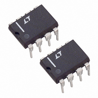
LTC1422CN8#PBF Linear Technology, LTC1422CN8#PBF Datasheet - Page 8

LTC1422CN8#PBF
Manufacturer Part Number
LTC1422CN8#PBF
Description
IC CONTROLLER HOT SWAP 8-DIP
Manufacturer
Linear Technology
Type
Hot-Swap Controllerr
Datasheet
1.LTC1422CS8PBF.pdf
(16 pages)
Specifications of LTC1422CN8#PBF
Applications
General Purpose
Internal Switch(s)
No
Voltage - Supply
2.7 V ~ 12 V
Operating Temperature
0°C ~ 70°C
Mounting Type
Through Hole
Package / Case
8-DIP (0.300", 7.62mm)
Lead Free Status / RoHS Status
Lead free / RoHS Compliant
APPLICATIONS
LTC1422
When the voltage at the FB pin rises above its reset
threshold (1.232V), the comparator COMP 2 output goes
high, and a timing cycle starts (Figure 4, time points 1 and
4). After a complete timing cycle, RESET is pulled high.
The 12 A pull-up current source to V
series diode so the pin can be pulled above V
external pull-up resistor without forcing current back into
supply.
When the supply voltage at the FB pin drops below its reset
threshold, the comparator Comp 2 output goes low. After
passing through a glitch filter, RESET is pulled low (time
point 2). If the FB pin rises above the reset threshold for
less than a timing cycle, the RESET output will remain low
(time point 3).
Glitch Filter
The LTC1422 has a glitch filter to prevent RESET from
generating a system reset when there are transients on the
FB pin. The filter is 20 s for large transients (greater than
150mV) and up to 80 s for small transients. The relation-
ship between glitch filter time and the transient voltage is
shown in Typical Performance curve: Glitch Filter Time vs
Feedback Transient.
Soft Reset
In some cases a system reset is desired without a power
down. The ON pin can signal the RESET pin to go low
without turning off the external N-channel (a soft reset).
This is accomplished by holding the ON pin low for only
15 s or less (Figure 5, time point 1). At about 30 s from
the falling edge of the ON pin (time point 2) the RESET pin
goes low and stays low for one timing cycle.
8
TIMER
RESET
V
OUT
V2
1
Figure 4. Supply Monitor Waveforms
1.232V
U
2
V1
INFORMATION
U
V2
3
V1
W
CC
V2
4
on RESET has a
U
CC
1.232V
1422 F04
by an
ON
If the ON pin is held low for longer than 30 s (typ), the gate
will turn off and the RESET pin will eventually go low (time
points 4, 5 and 6).
Timer
The system timing for the LTC1422 is generated by the
circuitry shown in Figure 6. The timer is used to set the
turn-on delay after the ON pin goes high and the delay
before the RESET pin goes high after the output supply
voltage is good as sensed by the FB pin.
2
TIMER
RESET
GATE
V
OUT
LTC1422
ON
V
TIMER
3
CC
1.232V
2 A
C2
1
Figure 6. System Timing Block Diagram
30 s
Figure 5. Soft Reset Waveforms
15 s
V
–
+
CC
2
8
COMP 4
R1
Q1
SENSE
7
LOGIC
3
GATE
30 s (typ)
Q2
6
R2
MONITOR
4
SUPPLY
4
C1
5
6
20 s
5
1
RESET
R3
R4
+
1422 F06
1422 F05
1422fb
V
C
OUT
LOAD


