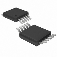
LTC4211CMS#TR Linear Technology, LTC4211CMS#TR Datasheet - Page 10

LTC4211CMS#TR
Manufacturer Part Number
LTC4211CMS#TR
Description
IC CONTROLLER HOT SWAP 10-MSOP
Manufacturer
Linear Technology
Type
Hot-Swap Controllerr
Datasheet
1.LTC4211IMS8PBF.pdf
(36 pages)
Specifications of LTC4211CMS#TR
Applications
General Purpose
Internal Switch(s)
No
Voltage - Supply
2.5 V ~ 16.5 V
Operating Temperature
0°C ~ 70°C
Mounting Type
Surface Mount
Package / Case
10-TFSOP, 10-MSOP (0.118", 3.00mm Width)
Linear Misc Type
Positive Low Voltage
Family Name
LTC4211
Package Type
MSOP
Operating Supply Voltage (min)
2.5V
Operating Supply Voltage (max)
16.5V
Operating Temperature (min)
0C
Operating Temperature (max)
70C
Operating Temperature Classification
Commercial
Product Depth (mm)
3mm
Product Height (mm)
0.86mm
Product Length (mm)
3mm
Mounting
Surface Mount
Pin Count
10
Lead Free Status / RoHS Status
Contains lead / RoHS non-compliant
Lead Free Status / RoHS Status
Contains lead / RoHS non-compliant
Other names
LTC4211CMSTR
Available stocks
Company
Part Number
Manufacturer
Quantity
Price
PI FU CTIO S
LTC4211
RESET (Pin 1/Pin 1): An open-drain N-channel MOSFET
whose source connects to GND (Pin 4/Pin 5). This pin
pulls low if the voltage at the FB pin (Pin 5/Pin 6) falls below
the FB pin threshold (1.236V). During the start-up cycle,
the RESET pin goes high impedance at the end of the
second timing cycle after the FB pin goes above the FB
threshold. This pin requires an external pull-up resistor to
V
RESET pin pulls low independently of the FB pin to prevent
false glitches.
ON (Pin 2/Pin 2): An active high signal used to enable or
disable LTC4211 operation. COMP1’s threshold is set at
1.236V and its hysteresis is set at 80mV. If a logic high
signal is applied to the ON pin (V
timing cycle begins if an overvoltage condition does not
exist on the GATE pin (Pin 6/Pin 7). If a logic low signal is
applied to the ON pin (V
pulled low by an internal 200µA current sink. The ON pin
can also be used to reset the electronic circuit breaker. If
the ON pin is cycled low and then high following a circuit
breaker trip, the internal circuit breaker is reset, and the
LTC4211 begins a new start-up cycle.
TIMER (Pin 3/Pin 4): A capacitor connected from this pin
to GND sets the LTC4211’s system timing. The LTC4211’s
initial and second start-up timing cycles and its internal
“power good” delay time are defined by this capacitor.
GND (Pin 4/Pin 5): Device Ground Connection. Connect
this pin to the system’s analog ground plane.
FB (Pin 5/Pin 6): The FB (Feedback) pin is an input to the
COMP2 comparator and monitors the output supply volt-
age through an external resistor divider. If V
the RESET pin pulls low. An internal glitch filter at COMP2’s
output helps prevent negative voltage transients from
triggering a reset condition. If V
goes high after one timing cycle.
GATE (Pin 6/Pin 7): The output signal at this pin is the
high side gate drive for the external N-channel FET pass
transistor.
10
CC
U
. If an undervoltage lockout condition occurs, the
U
U
ON
(8-Lead Package/10-Lead Package)
< 1.236V), the GATE pin is
FB
> 1.239V, the RESET pin
ON
> 1.316V), the first
FB
< 1.236V,
As shown in the Block Diagram, an internal charge pump
supplies a 10µA gate current and sufficient gate voltage
drive to the external FET for supply voltages from 2.5V to
16.5V. The internal charge-pump and zener clamps at the
GATE pin determine the gate drive voltage (∆V
V
of ∆V
For V
connecting between GATE and V
typically at 12V and with guaranteed minimum value of
10V. For V
for ∆V
typically. The minimum Z2’s clamp voltage is 23V. This
effectively sets ∆V
SENSE (Pin 7/Pin 8): Circuit Breaker Set Pin. With a sense
resistor placed in the power path between V
the LTC4211’s electronic circuit breaker trips if the voltage
across the sense resistor exceeds the thresholds set
internally for the SLOW COMP and the FAST COMP, as
shown in the Block Diagram. The threshold for the SLOW
COMP is V
breaker trips if the voltage across the sense resistor
exceeds 50mV for 20µs. The SLOW COMP delay is fixed in
the S8/MS8 version and adjustable in the MS version of
the LTC4211. To adjust the SLOW COMP’s delay, please
refer to the section on Adjusting SLOW COMP’s Response
Time.
Under transient conditions where large step current
changes can and do occur over shorter periods of time, a
second (fast) comparator instead trips the electronic
circuit breaker. The threshold for the FAST COMP is set at
V
voltage across the sense resistor exceeds 150mV for more
than 300ns. The FAST COMP’s delay is fixed in the
LTC4211 and cannot be adjusted. To disable the electronic
circuit breaker, connect the V
V
LTC4211. The LTC4211 operates from 2.5V < V
and the supply current is typically 1mA. An internal und-
ervoltage lockout circuit disables the device until the
voltage at V
GATE
CB(FAST)
CC
(Pin 8/Pin 9): This is the positive supply input to the
CC
GATE
– V
GATE
> 4.75V, the ∆V
CC
= 150mV, and the circuit breaker trips if the
for supplies in the range of 2.7V < V
CC
. Z2 clamps the gate voltage to ground to 26V
CB(SLOW)
). The charge pump produces a minimum 4.5V
CC
> 15V, the zener clamp Z2 sets the limitation
exceeds 2.3V.
GATE
= 50mV, and the electronic circuit
to 8V minimum.
GATE
is limited by zener clamp Z1
CC
and SENSE pins together.
CC
pins. The ∆V
CC
and SENSE,
CC
CC
< 4.75V.
< 16.5V,
GATE
GATE
4211fa
is
=


