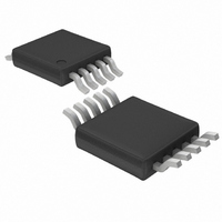
LTC4211CMS#TR Linear Technology, LTC4211CMS#TR Datasheet - Page 22

LTC4211CMS#TR
Manufacturer Part Number
LTC4211CMS#TR
Description
IC CONTROLLER HOT SWAP 10-MSOP
Manufacturer
Linear Technology
Type
Hot-Swap Controllerr
Datasheet
1.LTC4211IMS8PBF.pdf
(36 pages)
Specifications of LTC4211CMS#TR
Applications
General Purpose
Internal Switch(s)
No
Voltage - Supply
2.5 V ~ 16.5 V
Operating Temperature
0°C ~ 70°C
Mounting Type
Surface Mount
Package / Case
10-TFSOP, 10-MSOP (0.118", 3.00mm Width)
Linear Misc Type
Positive Low Voltage
Family Name
LTC4211
Package Type
MSOP
Operating Supply Voltage (min)
2.5V
Operating Supply Voltage (max)
16.5V
Operating Temperature (min)
0C
Operating Temperature (max)
70C
Operating Temperature Classification
Commercial
Product Depth (mm)
3mm
Product Height (mm)
0.86mm
Product Length (mm)
3mm
Mounting
Surface Mount
Pin Count
10
Lead Free Status / RoHS Status
Contains lead / RoHS non-compliant
Lead Free Status / RoHS Status
Contains lead / RoHS non-compliant
Other names
LTC4211CMSTR
Available stocks
Company
Part Number
Manufacturer
Quantity
Price
OPERATIO
LTC4211
The maximum load current that trips the circuit breaker is
given in Equation 12.
where
For example:
If a sense resistor with 7mΩ ±5% R
limiting, the nominal trip current I
Equations 11 and 12, I
9.02A respectively.
For proper operation and to avoid the circuit breaker
tripping unnecessarily, the minimum trip current
(I
load current. For reliability purposes, the operation at the
maximum trip current (I
carefully. If necessary, two resistors with the same R
can be connected in parallel to yield an R
that fits the circuit requirements.
POWER MOSFET SELECTION CRITERIA
To start the power MOSFET selection process, choose the
maximum drain-to-source voltage, V
maximum drain current, I
V
voltage (including surges, spikes, ringing, etc.) and the
I
current in the system during a fault condition. In addition,
consider three other key parameters: 1) the required gate-
source (V
drain-to-source on resistance, R
mum junction temperature rating of the MOSFET.
22
D(MAX)
DS(MAX)
TRIP(MIN)
I
TRIP MAX
R
SENSE MIN
(
rating must exceed the maximum short-circuit
GS
rating must exceed the maximum input supply
) must exceed the circuit’s maximum operating
(
) voltage drive, 2) the voltage drop across the
)
=
)
R
=
U
V
SENSE MIN
R
CB MAX
SENSE NOM
(
TRIP(MIN)
(
(
TRIP(MAX)
)
D(MAX)
)
=
)
• –
R
= 5.4A and I
DS(ON)
⎡
⎢
⎣
SENSE MIN
TRIP(NOM)
1
60
TOL
of the MOSFET. The
) must be evaluated
⎛
⎝ ⎜
mV
R
is used for current
(
DS(MAX)
100 ⎦ ⎦ ⎥
SENSE(NOM)
and 3) the maxi-
TOL
)
= 7.1A. From
⎞
⎠ ⎟
TRIP(MAX)
⎤
, and the
value
(12)
TOL
=
Power MOSFETs are classified into two categories: stan-
dard MOSFETs (R
logic-level MOSFETs (R
sub-logic-level MOSFETs (R
The absolute maximum rating for V
standard MOSFETs. However, the V
for logic-level MOSFETs ranges from ±8V to ±20V de-
pending upon the manufacturer and the specific part
number. The LTC4211’s GATE overdrive as a function of
V
level and sub-logic-level MOSFETs are recommended for
low supply voltage applications and standard MOSFETs
can be used for applications where supply voltage is
greater than 4.75V.
Note that in some applications, the gate of the external
MOSFET can discharge faster than the output voltage
when the circuit breaker is tripped. This causes a negative
V
external MOSFET should have a ±V
higher than the operating input supply voltage to ensure
that the external MOSFET is not destroyed by a negative
V
MOSFET must be higher than the gate overdrive voltage.
Lower ±V
LTC4211 if the GATE overdrive is clamped to a lower
voltage. The circuit in Figure 12 illustrates the use of Zener
diodes to clamp the LTC4211’s GATE overdrive signal if
lower voltage MOSFETs are used.
CC
GS
GS
Figure 12. Optional Gate Clamp for Lower V
is illustrated in the Typical Performance curves. Logic-
voltage on the external MOSFET. Usually, the selected
voltage. In addition, the ±V
*USER SELECTED VOLTAGE CLAMP
(A LOW BIAS CURRENT ZENER DIODE IS RECOMMENDED)
1N4688 (5V)
1N4692 (7V): LOGIC-LEVEL MOSFET
1N4695 (9V)
1N4702 (15V): STANDARD-LEVEL MOSFET
V
GS(MAX)
CC
R
SENSE
rating MOSFETs can be used with the
DS(ON)
DS(ON)
GATE
Q1
DS(ON)
R
200Ω
specified at V
G
D1*
specified at V
specified at V
GS
GS(MAX)
D2*
GS(MAX)
GS
is typically ±20V for
GS(MAX)
maximum rating
rating of the
GS
4211 F12
rating that is
V
GS
OUT
GS
= 5V), and
MOSFETs
= 10V)
= 2.5V).
4211fa


