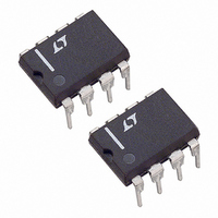
LTC1422IN8#PBF Linear Technology, LTC1422IN8#PBF Datasheet - Page 10

LTC1422IN8#PBF
Manufacturer Part Number
LTC1422IN8#PBF
Description
IC CONTROLLER HOT SWAP 8-DIP
Manufacturer
Linear Technology
Type
Hot-Swap Controllerr
Datasheet
1.LTC1422CS8PBF.pdf
(16 pages)
Specifications of LTC1422IN8#PBF
Applications
General Purpose
Internal Switch(s)
No
Voltage - Supply
2.7 V ~ 12 V
Operating Temperature
-40°C ~ 85°C
Mounting Type
Through Hole
Package / Case
8-DIP (0.300", 7.62mm)
Lead Free Status / RoHS Status
Lead free / RoHS Compliant
Available stocks
Company
Part Number
Manufacturer
Quantity
Price
LTC1422
APPLICATIONS
and C3 are used to set the rise and fall delays on the 5V
supply. Next, the 3.3V supply ramps up with a 20ms delay
set by R6 and C2. On the falling edge, the 3.3V supply
ramps down first because R6 is bypassed by the diode D1.
Using the LTC1422 as a Linear Regulator
The LTC1422 can be used to Hot Swap the primary supply
and generate a secondary low dropout regulated supply.
Figure 11 shows how to switch a 5V supply and create a
3.3V supply using the reset comparator and one addi-
tional transistor. The FB pin is used to monitor the 3.3V
output. When the voltage on the gate of Q2 increases, the
3.3V increases. At the 3.3V threshold, the reset compara-
tor will trip. The RESET pin goes high which turns on Q3.
This lowers the voltage on the gate of Q2. This feedback
loop is compensated by the capacitor C1 and the resistors
R6 and R7.
10
U
ON/RESET
V
INFORMATION
CC
U
3.3V
V
V
5V
IN
IN
C1
0.33 F
16V
CURRENT LIMIT: 5A
RESET
ON
W
1
2
3
4
RESET
ON
TIMER
GND
LTC1422
3.3V OUT
10k
5V OUT
SENSE
GATE
V
Figure 10. Switching 5V and 3.3V
CC
FB
10k
U
8
7
6
5
Q4
Q2: 2N7002LT1
Q3, Q4: MMBT3904LT1
Figure 9. ON Pin Circuitry
0.01
Q3
5%
R2
10k
Q2
1/2 Si9436
2
C3
0.047 F
25V
Q1
ON
TIMER
R3
10
5%
R1
10k
5%
V
Hot Swapping 48V DC/DC Module with
Active Low On/Off Control Signal
Using a 7.5V Zener and a resistor, the LTC1422 can switch
supplies much greater than the 12V V
shown in Figure 12, the switching FET Q1 is connected as
a common source driver rather than the usual source
follower used in previous applications. This allows the
ground of the LTC1422 to sit at the negative terminal of the
48V input. The clamp circuit of R5 and D1 provides power
to the LTC1422. The resistive divider R1 and R2 at the ON
pin monitors the input supply. The switching FET Q1 is
prevented from turning on until the input supply is at least
38V. Using the reset comparator to monitor the gate
voltage allows the module to be turned on after the gate
has reached a minimum level plus one timing cycle. A high
voltage transistor Q2 is used to translate the RESET signal
to the module On/Off input.
CC
3
8
REF
C2
1N4148
D1
5%
R1
R6
1M
+
–
1/2 Si99436
COMP 5
SENSE
Q2
R7
10
5%
7
C2
0.022 F
25V
LOGIC
GATE
Q1
LTC1422
4
6
R2
R4
2.74k
1%
R5
1k
1%
FB
+
+
TRIP POINT: 4.6V
5
1
C
C
LOAD
LOAD
RESET
C1
1422 F10
V
3.3V
V
5V
R4
OUT
OUT
R3
+
1422 F09
C
V
LOAD
OUT
CC
pin rating. As
1422fb


