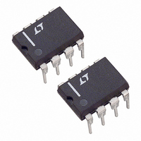
LTC1422IN8#PBF Linear Technology, LTC1422IN8#PBF Datasheet - Page 7

LTC1422IN8#PBF
Manufacturer Part Number
LTC1422IN8#PBF
Description
IC CONTROLLER HOT SWAP 8-DIP
Manufacturer
Linear Technology
Type
Hot-Swap Controllerr
Datasheet
1.LTC1422CS8PBF.pdf
(16 pages)
Specifications of LTC1422IN8#PBF
Applications
General Purpose
Internal Switch(s)
No
Voltage - Supply
2.7 V ~ 12 V
Operating Temperature
-40°C ~ 85°C
Mounting Type
Through Hole
Package / Case
8-DIP (0.300", 7.62mm)
Lead Free Status / RoHS Status
Lead free / RoHS Compliant
Available stocks
Company
Part Number
Manufacturer
Quantity
Price
APPLICATIONS
Hot Circuit Insertion
When circuit boards are inserted into a live backplane, the
supply bypass capacitors on the board can draw huge
transient currents from the backplane power bus as they
charge up. The transient currents can cause permanent
damage to the connector pins and cause glitches on the
system supply, causing other boards in the system to
reset.
The LTC1422 is designed to turn a board’s supply voltage
on and off in a controlled manner, allowing the board to be
safely inserted or removed from a live backplane. The chip
also provides a system reset signal to indicate when board
supply voltage drops below a programmable voltage.
Power Supply Ramping
The onboard power supply is controlled by placing an
external N-channel pass transistor in the power path
(Figure 1). R1 provides current fault detection and R2
prevents high frequency oscillation. By ramping up the
gate of the pass transistor at a controlled rate, the transient
surge current (I = C • dV/dt) drawn from the main backplane
supply can be limited to a safe value when the board makes
connection.
When power is first applied to the chip, the gate of the
N-channel (Pin 6) is pulled low. After the ON pin is held
high for at least one timing cycle, the charge pump is
turned on. The voltage at GATE begins to rise with a slope
V
CC
2
Figure 1. Supply Control Circuitry
V
ON
TIMER
CC
8
R1
3
LTC1422
U
SENSE
C2
7
RESET
GND
GATE
INFORMATION
Q1
U
4
FB
6
R2
10
5
1
C1
W
R3
R4
+
C
1422F01
LOAD
V
U
OUT
ON
equal to 10 A/C1 (Figure 2), where C1 is the external
capacitor connected between the GATE pin and GND.
The ramp time for the supply is equal to: t = (V
10 A. After the ON pin has been pulled low for more than
40 s, the GATE is immediately pulled to GND.
Voltage Monitor
The LTC1422 uses a 1.232V bandgap reference, precision
voltage comparator and a resistive divider to monitor the
output supply voltage (Figure 3).
2
V
LTC1422
CC
V
+ 10V
CC
TIMER
LOGIC
V
CC
Figure 3. Supply Monitor Block Diagram
3
C2
V
CC
Figure 2. Supply Turn-On
8
R1
REFERENCE
SLOPE = 10 A/C1
COMP 2
SENSE
1.232V
t
7
1
+
–
GATE
Q1
6
R2
Q2
4
12 A
C1
FB
t
LTC1422
5
1
2
1422 F03
R3
R4
RESET
CC
P
+
GATE
V
OUT
• C1)/
1422 F02
1422fb
V
7
C
OUT
LOAD


