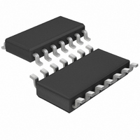
LTC1645CS Linear Technology, LTC1645CS Datasheet - Page 18

LTC1645CS
Manufacturer Part Number
LTC1645CS
Description
IC CTRLR SEQ HOTSWAP DUAL 14SOIC
Manufacturer
Linear Technology
Type
Hot-Swap Controllerr
Datasheet
1.LTC1645CS8PBF.pdf
(24 pages)
Specifications of LTC1645CS
Applications
General Purpose
Internal Switch(s)
No
Voltage - Supply
1.2 V ~ 12 V
Operating Temperature
0°C ~ 70°C
Mounting Type
Surface Mount
Package / Case
14-SOIC (0.154", 3.90mm Width)
Linear Misc Type
Positive Low Voltage
Family Name
LTC1645
Package Type
SOIC N
Operating Supply Voltage (min)
1.2V
Operating Supply Voltage (max)
12V
Operating Temperature (min)
0C
Operating Temperature (max)
70C
Operating Temperature Classification
Commercial
Product Depth (mm)
3.99mm
Product Height (mm)
1.5mm
Mounting
Surface Mount
Pin Count
14
Lead Free Status / RoHS Status
Contains lead / RoHS non-compliant
Lead Free Status / RoHS Status
Contains lead / RoHS non-compliant
Available stocks
Company
Part Number
Manufacturer
Quantity
Price
Part Number:
LTC1645CS
Manufacturer:
LINEAR/凌特
Quantity:
20 000
Part Number:
LTC1645CS#TRPBF
Manufacturer:
LINEAR/凌特
Quantity:
20 000
Part Number:
LTC1645CS8
Manufacturer:
LINEAR/凌特
Quantity:
20 000
Part Number:
LTC1645CS8#TRPBF
Manufacturer:
LT/凌特
Quantity:
20 000
APPLICATIO S I FOR ATIO
LTC1645
Switching Regulator Supply Sequencing
Figure 21 shows the LTC1645 sequencing two power
supplies, the lower of which is generated by the LTC1430A
switching regulator. Connecting the regulator’s FB pin
resistor divider (R1 and R2) to the other side of the pass
FET (Q1) allows the LTC1430A to compensate for the
voltage drop across R
voltage output. The spare comparator holds the LTC1645’s
ON pin low until the LTC1430A’s output is at least 3V, and
shuts both channels off if it drops below 3V. When the
ON/OFF signal is taken high to 5V (turn-on), the voltage at
the ON pin rises with an RC exponential characteristic,
reaching 0.8V first. This starts a timing cycle, and GATE1
begins to rise. GATE2 starts to ramp up after the ON pin
reaches 2V. As long as the timing cycle is shorter than the
time for the ON pin to rise from 0.8V to 2V, V
up after V
V
low, the voltage at the ON pin exponentially decays and
GATE2 ramps down before GATE1. RESET goes low as
soon as V
up and power-down sequences of the circuit in Figure 21.
18
OUT1
exceeds 3V. When the ON/OFF signal is brought
OUT1
OUT1
falls below 3V. Figure 22 shows the power-
. RESET goes high one timing cycle after
U
SENSE1
U
2V/DIV
2V/DIV
5V/DIV
and Q1, assuring an accurate
RESET
V
V
V
2V/DIV
2V/DIV
REGOUT
OUT1
OUT2
ON
Figure 22. Switching Regulator Supply Sequencing
W
OUT2
U
ramps
Switching Regulator Hot Swapping
High current switching regulators usually require large
bypass capacitors on both input and output for proper
operation. The application in Figure 23 controls the inrush
current to the LTC1649’s input bypass capacitors and
ramps the two output voltages up and down together. As
with the previous application, connecting the regulator’s
FB pin resistor divider to the other side of the output pass
FET (Q2) allows the LTC1649 to compensate for the
voltage drop across Q2, assuring an accurate voltage
output. The voltage at the LTC1645’s ON pin reaches 0.8V
when V
timing cycle later. As the regulator’s output rises, D2 pulls
the ON pin above 2V and GATE2 begins to rise, ramping
V
cycle after V
Figure 24 shows the circuit in Figure 23 powering up.
Care should be taken connecting a switching regulator’s
FB or SENSE pins to a node other than its output. Depend-
ing on the regulator’s internal architecture, unusual be-
havior may occur as it tries in vain to raise the voltage at
OUT1
and V
IN
exceeds 3V, and GATE1 begins to ramp up one
OUT2
OUT1
up together. RESET goes high one timing
exceeds 3V and V
OUT2
exceeds 2.35V.
1645fa


