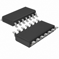
LTC1645CS Linear Technology, LTC1645CS Datasheet - Page 21

LTC1645CS
Manufacturer Part Number
LTC1645CS
Description
IC CTRLR SEQ HOTSWAP DUAL 14SOIC
Manufacturer
Linear Technology
Type
Hot-Swap Controllerr
Datasheet
1.LTC1645CS8PBF.pdf
(24 pages)
Specifications of LTC1645CS
Applications
General Purpose
Internal Switch(s)
No
Voltage - Supply
1.2 V ~ 12 V
Operating Temperature
0°C ~ 70°C
Mounting Type
Surface Mount
Package / Case
14-SOIC (0.154", 3.90mm Width)
Linear Misc Type
Positive Low Voltage
Family Name
LTC1645
Package Type
SOIC N
Operating Supply Voltage (min)
1.2V
Operating Supply Voltage (max)
12V
Operating Temperature (min)
0C
Operating Temperature (max)
70C
Operating Temperature Classification
Commercial
Product Depth (mm)
3.99mm
Product Height (mm)
1.5mm
Mounting
Surface Mount
Pin Count
14
Lead Free Status / RoHS Status
Contains lead / RoHS non-compliant
Lead Free Status / RoHS Status
Contains lead / RoHS non-compliant
Available stocks
Company
Part Number
Manufacturer
Quantity
Price
Part Number:
LTC1645CS
Manufacturer:
LINEAR/凌特
Quantity:
20 000
Part Number:
LTC1645CS#TRPBF
Manufacturer:
LINEAR/凌特
Quantity:
20 000
Part Number:
LTC1645CS8
Manufacturer:
LINEAR/凌特
Quantity:
20 000
Part Number:
LTC1645CS8#TRPBF
Manufacturer:
LT/凌特
Quantity:
20 000
APPLICATIO S I FOR ATIO
its FB or SENSE pin. In the case of the LTC1649, large peak
currents result if the FB pin is at ground and not connected
directly to the output inductor and capacitors. To keep the
peak currents under control, R1, R2 and D1 hold the FB pin
above ground but below its normal regulated value until
V
Power N-Channel Selection
The R
enough so that the voltage drop across them is 100mV or
less at full current. If the R
drop across the transistor can cause the output voltage to
trip the reset circuit. The transistors listed in Table 1 or
other similar transistors are recommended for use with
the LTC1645.
Low voltage applications may require the use of logic-level
FETs; ensure their maximum V
application. GATE voltage as a function of V
in the Typical Performance curves. If lower GATE drive is
desired, connect a diode in series with a zener between
GATE and V
Figure 25.
V
2V/DIV
2V/DIV
REGOUT
2V/DIV
2V/DIV
2V/DIV
5V/DIV
RESET
V
OUT2
V
V
REGIN
OUT2
OUT1
ON
DS(ON)
ramps up and D1 reverse-biases.
CC
of the external pass transistors must be low
Figure 24. Switching Regulator Hot Swap
or between GATE and V
U
U
DS(ON)
GS
rating is sufficient for the
is too high, the voltage
W
OUT
CC
as shown in
is illustrated
U
Table 1. N-Channel Selection Guide
10A to 20A
10A to 20A
CURRENT
5A to 10A
5A to 10A
5A to 10A
5A to 10A
1A to 2A
1A to 2A
2A to 5A
2A to 5A
LEVEL
V
CC
SUB75N03-04
*USER SELECTED VOLTAGE CLAMP
1N4688 (5V)
1N4692 (7V): LOGIC-LEVEL MOSFET
1N4695 (9V)
1N4702 (15V): STANDARD-LEVEL MOSFET
NDH8503N
MMSF3300
Si6928DQ
FDB8030L
Si4920DY
NUMBER
FDS6680
Figure 25. Optional Gate Clamp
IRF7313
IRF7413
Si4420
PART
D1*
R1
1N4148
D2
ON Semiconductor
MANUFACTURER
Vishay/Siliconix
Vishay/Siliconix
Vishay/Siliconix
Vishay/Siliconix
Q1
International
International
Fairchild
Rectifier
Fairchild
Rectifier
Fairchild
1N4148
D2
D4*
LTC1645
DESCRIPTION
Dual N-Channel
R
SuperSOT-8
Dual N-Channel
R
TSSOP-8
Dual N-Channel
R
SO-8
Dual N-Channel
R
SuperSOT-8
Single N-Channel
R
SO-8
Single N-Channel
R
SO-8
Single N-Channel
R
SO-8
Single N-Channel
R
SO-8
Single N-Channel
R
TO-263AB
Single N-Channel
R
D
DS(ON)
DS(ON)
DS(ON)
DS(ON)
DS(ON)
DS(ON)
DS(ON)
DS(ON)
DS(ON)
DS(ON)
2
PAK
1645 F25
V
OUT
= 0.033
= 0.035
= 0.025
= 0.029
= 0.009
= 0.01
= 0.011
= 0.0125
= 0.0035
= 0.004
21
1645fa


