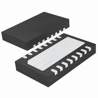
LTC4217CDHC-12#TRPBF Linear Technology, LTC4217CDHC-12#TRPBF Datasheet - Page 12

LTC4217CDHC-12#TRPBF
Manufacturer Part Number
LTC4217CDHC-12#TRPBF
Description
IC CTRLR HOT SWAP 2A 16-DFN
Manufacturer
Linear Technology
Type
Hot-Swap Switchr
Datasheet
1.LTC4217IFEPBF.pdf
(18 pages)
Specifications of LTC4217CDHC-12#TRPBF
Applications
General Purpose
Internal Switch(s)
Yes
Current Limit
2.0A
Voltage - Supply
2.9 V ~ 26.5 V
Operating Temperature
0°C ~ 70°C
Mounting Type
Surface Mount
Package / Case
16-WFDFN Exposed Pad
Lead Free Status / RoHS Status
Lead free / RoHS Compliant
Available stocks
Company
Part Number
Manufacturer
Quantity
Price
APPLICATIONS INFORMATION
LTC4217
a resistor between the I
the Functional Diagram the voltage at the I
the clamp circuit) sets the CS amplifier’s built-in offset
voltage. This offset voltage directly determines the active
current limit value. With the I
the I
efficient reference. This voltage is set to 0.618V at room
temperature which corresponds to a 2A current limit at
room temperature.
An external resistor placed between the I
forms a resistive divider with the internal 20k sourcing
resistor. The divider acts to lower the voltage at the I
pin and therefore lower the current limit threshold. The
overall current limit threshold precision is reduced to
±16% when using a 20k resistor to halve the threshold.
Using a switch (connected to ground) in series with this
external resistor allows the active current limit to change
only when the switch is closed. This feature can be used
when the start-up current exceeds the typical maximum
load current.
Monitor MOSFET Temperature
The voltage at the I
ing temperature. The temperature profile of the I
shown in the Typical Performance Characteristics section.
Using a comparator or ADC to measure the I
provides an indicator of the MOSFET temperature.
There is an overtemperature circuit in the LTC4217 that
monitors an internal voltage similar to the I
When the die temperature exceeds 145°C the circuit turns
off the MOSFET until the temperature drops to 125°C.
Monitor MOSFET Current
The current in the MOSFET passes through a sense resistor.
The voltage on the sense resistor is converted to a cur-
rent that is sourced out of the I
amplifier is 50µA/A from I
This output current can be converted to a voltage using an
external resistor to drive a comparator or ADC. The voltage
compliance for the I
A microcontroller with a built-in comparator can build a
simple integrating single-slope ADC by resetting a capaci-
12
SET
pin is determined by a positive temperature co-
SET
MON
pin increases linearly with increas-
SET
pin is from 0V to INTV
MON
pin and ground. As shown in
SET
MON
for 1A of MOSFET current.
pin open, the voltage at
pin. The gain of I
SET
SET
pin and ground
SET
pin voltage.
SET
CC
SET
pin (via
voltage
– 0.7V.
SENSE
pin is
SET
tor that is charged with this current. When the capacitor
voltage trips the comparator and the capacitor is reset, a
timer is started. The time between resets will indicate the
MOSFET current.
Monitor OV and UV Faults
Protecting the load from an overvoltage condition is
the main function of the OV pin. In the LTC4217-12, an
internal resistive divider (driving the OV pin) connects
to a comparator to turn off the MOSFET when the V
voltage exceeds 15.05V. If the V
back below 14.8V, the switch will be allowed to turn on
immediately. In the LTC4217 the OV pin threshold is 1.23V
when rising, and 1.21V when falling out of overvoltage.
The UV pin functions as an undervoltage protection pin or
as an “ON” pin. In the LTC4217-12 the MOSFET turns off
when V
rises above 9.88V for 100ms, the switch will be allowed
to turn on again. The LTC4217 UV turn-on/off thresholds
are 1.23V (rising) and 1.15V (falling).
In the cases of an undervoltage or overvoltage the MOSFET
turns off and there is indication on the PG status pin. When
the overvoltage is removed the MOSFET’s gate ramps up
immediately at the rate determined by the INRUSH block.
Power Good Indication
In addition to setting the foldback current limit threshold,
the FB pin is used to determine a power good condition.
The LTC4217-12 uses an internal resistive divider on the
OUT pin to drive the FB pin. The PG comparator indicates
logic high when OUT pin rises above 10.5V. If the OUT pin
subsequently falls below 10.3V the comparator toggles low.
On the LTC4217 the PG comparator drives high when the
FB pin rises above 1.23V and low when falls below 1.21V.
Once the PG comparator is high the GATE pin voltage is
monitored with respect to the OUT pin. Once the GATE
minus OUT voltage exceeds 4.2V the PG pin goes high.
This indicates to the system that it is safe to load the OUT
pin while the MOSFET is completely turned “on”. The PG
pin goes low when the GATE is commanded off (using
the UV, OV or SENSE pins) or when the PG comparator
drives low.
DD
falls below 9.23V. If the V
DD
pin subsequently falls
DD
pin subsequently
4217fd
DD


