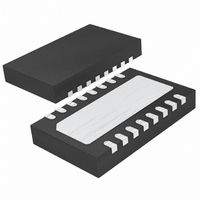
LTC4217CDHC-12#TRPBF Linear Technology, LTC4217CDHC-12#TRPBF Datasheet - Page 13

LTC4217CDHC-12#TRPBF
Manufacturer Part Number
LTC4217CDHC-12#TRPBF
Description
IC CTRLR HOT SWAP 2A 16-DFN
Manufacturer
Linear Technology
Type
Hot-Swap Switchr
Datasheet
1.LTC4217IFEPBF.pdf
(18 pages)
Specifications of LTC4217CDHC-12#TRPBF
Applications
General Purpose
Internal Switch(s)
Yes
Current Limit
2.0A
Voltage - Supply
2.9 V ~ 26.5 V
Operating Temperature
0°C ~ 70°C
Mounting Type
Surface Mount
Package / Case
16-WFDFN Exposed Pad
Lead Free Status / RoHS Status
Lead free / RoHS Compliant
Available stocks
Company
Part Number
Manufacturer
Quantity
Price
APPLICATIONS INFORMATION
12V Fixed Version
In the LTC4217-12 the UV, OV and FB pins are driven by
internal dividers which may need to be filtered to prevent
false faults. By placing a bypass capacitor on these pins
the faults are delayed by the RC time constant. Use the
R
calculation.
In cases where the fixed thresholds need a slight adjust-
ment, placing a resistor from the UV or OV pins to V
or GND will adjust the threshold up or down. Likewise
placing a resistor between FB pin to OUT or GND adjusts
the threshold. Again use the R
characteristics table for this calculation.
An example in Figure 5 raises the UV turn-on voltage from
9.88V to 10.5V. Increasing the UV level requires adding a
resistor between UV and ground. The resistor, R
be calculated using electrical table parameters as follows:
In this same figure the OV threshold is lowered from
15.05V to 13.5V. Decreasing the OV threshold requires
adding a resistor between V
be calculated as follows:
IN
R
R
18k • 15.05
value from the electrical characteristics table for this
SHUNT1
SHUNT2
1.235
Figure 5. Adjusting LTC4217-12 Thresholds
=
=
(
R
V
R
( ) • V
NEW
IN
(
(
( ) • V
13.5 – 1.235
15.05 – 13.5
IN
V
( )
TH
LTC4217-12
– V
OLD
OLD
OLD
4217 F05
DD
)
(
V
=
(
IN
)
)
V
OV
UV
NEW
V
and OV. This resistor can
DD
(
OLD
value from the electrical
10.5 – 9.88
= 1.736M
18k • 9.88
R
R
– V
SHUNT2
SHUNT1
– V
OV TH
NEW
( )
)
)
SHUNT1
)
= 287k
=
, can
DD
The inrush current is defined by the current required to
charge the output capacitor using the fixed 0.3V/ms GATE
charge-up rate. The inrush current is defined as:
As mentioned previously the charge-up time is the out-
put voltage (12V) divided by the output rate of 0.3V/ms
resulting in 40ms. The peak power dissipation of 12V at
100mA (or 1.2W) is within the SOA of the pass MOSFET
for 40ms (see MOSFET SOA curve in the Typical Perfor-
mance Characteristics section).
Next the power dissipated in the MOSFET during overcurrent
must be limited. The active current limit uses a timer to
prevent excessive energy dissipation in the MOSFET. The
worst-case power dissipation occurs when the voltage
versus current profile of the foldback current limit is at
the maximum. This occurs when the current is 2A and the
voltage is one half of the 12V or 6V. See the Current Limit
Sense Voltage vs FB Voltage in the Typical Performance
Characteristics section to view this profile. In order to
survive 12W, the MOSFET SOA dictates a maximum time
of 10ms (see SOA graph). Use the internal 2ms timer
Use the equation for R
FB thresholds. Likewise use the equation for R
decreasing the UV and FB thresholds.
Design Example
Consider the following design example (Figure 6): V
12V, I
9.88V, V
triggers an automatic restart of the power-up sequence.
12V
I
INRUSH
MAX
OVOFF
Figure 6. 1.5A, 12V Card Resident Application
= 2A. I
= C
= 15.05V, V
L
•
INRUSH
0.1µF
0.3V
ms
C1
SHUNT1
PWRGD
= 100mA, C
= 330µF •
V
UV
FLT
TIMER
INTV
LTC4217-12DHC
DD
CC
for increasing the OV and
= 10.5V. A current limit fault
GND
I
OUT
MON
PG
L
0.3V
ms
= 330µF , V
12V
LTC4217
R1
10k
R2
20k
+
= 100mA
SHUNT2
C
330µF
L
13
UVON
ADC
4217fd
V
12V
1.5A
IN
OUT
4217 F06
for
=
=


