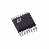
LTC1642IGN Linear Technology, LTC1642IGN Datasheet - Page 13

LTC1642IGN
Manufacturer Part Number
LTC1642IGN
Description
IC CONTROLLER HOTSWAP ADJ 16SSOP
Manufacturer
Linear Technology
Type
Hot-Swap Controllerr
Specifications of LTC1642IGN
Applications
General Purpose, Infiniband™
Internal Switch(s)
No
Voltage - Supply
2.97 V ~ 16.5 V
Operating Temperature
-40°C ~ 85°C
Mounting Type
Surface Mount
Package / Case
16-SSOP (0.150", 3.90mm Width)
Lead Free Status / RoHS Status
Contains lead / RoHS non-compliant
APPLICATIO S I FOR ATIO
Automatic Restart
If there is an overvoltage, and the resistor divider feeding
OV is connected to the output of the N-Channel pass
transistor, the LTC1642 will automatically restart even if
FAULT is not tied to ON. If the divider is connected to the
input side, the LTC1642 will restart itself only if FAULT is
tied to ON, and only after the overvoltage clears.
The OV and FB Comparators
The propagation delay through the OV and FB compara-
tors on low to high transitions depends strongly on the
differential input voltage. The relationship is shown in
Figure 11. The minimum propagation delay for large
overdrives is about 20µs. In addition the comparators
have 3mV of hysteresis.
Internal Voltage Clamp Protection
The LTC1642 includes a shunt regulator to protect itself
from V
turns on when V
chip’s circuitry to 15V. When it is on the chip functions
normally with one exception: if the charge pump is on, the
GATE voltage is usually near ground but this is not
guaranteed. Use the OV pin to ensure that GATE is grounded.
RST TMR
CRWBR
FAULT
GATE
OUT
CC
OV
IN
Figure 10. Overvoltage Timing (Output Side)
and SENSE pin voltages up to 33V. The regulator
CC
exceeds 16.5V and limits most of the
U
U
100ms/DIV
W
1642 F10
U
20V/DIV
2V/DIV
20V/DIV
20V/DIV
2V/DIV
2V/DIV
20V/DIV
The pull-up voltage on the RESET and FAULT pins follows
V
is on the pull-up voltage is 14.4V.
Undervoltage Monitor
The LTC1642 will assert RESET if a monitored voltage falls
below an adjustable minimum. When the monitored volt-
age has exceeded its minimum for at least one system
timing cycle, RESET goes high. The monitoring circuitry
comprises an internal 1.22V bandgap reference, an inter-
nal precision voltage comparator and an external resistive
divider to monitor the output supply voltage.
The circuit is shown in Figure 12, and typical waveforms
in Figure 13. When the voltage at the FB pin rises above its
reset threshold (1.22V), the comparator output goes low
and a timing cycle starts (times 1 and 5). Following the
cycle RESET is pulled high. At time 2 the voltage at FB
drops below the comparator’s threshold and RESET is
pulled low. If the FB pin rises above the reset threshold for
less than a timing cycle the RESET output will remain low
(time 3 to time 4). The 15µA pull-up current source to V
on RESET has a series diode so the pin can be pulled above
V
back into the supply.
CC
CC
until the shunt regulator turns on. When the regulator
by an external pull-up resistor without forcing current
Figure 11. OV Comparator Propagation Delay vs
Overdrive Voltage
70
60
50
40
30
20
10
0
0
40
OV OVERDRIVE (mV)
80
120
160
200
LTC1642
1642 F11
240
13
1642fb
CC


