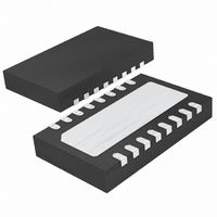
LTC4217CDHC#PBF Linear Technology, LTC4217CDHC#PBF Datasheet - Page 10

LTC4217CDHC#PBF
Manufacturer Part Number
LTC4217CDHC#PBF
Description
IC CTRLR HOT SWAP 2A 16-DFN
Manufacturer
Linear Technology
Type
Hot-Swap Switchr
Datasheet
1.LTC4217IFEPBF.pdf
(18 pages)
Specifications of LTC4217CDHC#PBF
Applications
General Purpose
Internal Switch(s)
Yes
Current Limit
2.0A
Voltage - Supply
2.9 V ~ 26.5 V
Operating Temperature
0°C ~ 70°C
Mounting Type
Surface Mount
Package / Case
16-WFDFN Exposed Pad
Linear Misc Type
Positive Low Voltage
Package Type
DFN EP
Operating Supply Voltage (min)
2.9V
Operating Temperature (min)
0C
Operating Temperature (max)
70C
Operating Temperature Classification
Commercial
Product Depth (mm)
3mm
Product Length (mm)
5mm
Mounting
Surface Mount
Pin Count
16
Lead Free Status / RoHS Status
Lead free / RoHS Compliant
Available stocks
Company
Part Number
Manufacturer
Quantity
Price
APPLICATIONS INFORMATION
LTC4217
After the power-on-reset pulse, the LTC4217 will go through
the following sequence. First, the UV and OV pins must
indicate that the input voltage is within the acceptable range.
All of these conditions must be satisfied for the duration
of 100ms to ensure that any contact bounce during the
insertion has ended.
The MOSFET is turned on by charging up the GATE with
a charge pump generated current source whose value is
adjusted by shunting a portion of the pull-up current to
ground. The charging current is controlled by the INRUSH
circuit that maintains a constant slope of GATE voltage ver-
sus time (Figure 2). The voltage at the GATE pin rises with
a slope of 0.3V/ms and the supply inrush current is set at:
This gate slope is designed to charge up a 1000µF ca-
pacitor to 12V in 40ms, with an inrush current of 300mA.
This allows the inrush current to stay under the current
limit threshold (500mA) for capacitors less than 1000µF .
Included in the Typical Performance Characteristics section
is a graph of the Safe Operating Area for the MOSFET. It is
10
12V
I
INRUSH
V
DD
Figure 1. 0.8A, 12V Card Resident Application
+ 6.15
= C
V
DD
L
0.1µF
C
• (0.3V/ms)
224k
T
20k
R1
R2
Figure 2. Supply Turn-On
0.1µF
C1
SLOPE = 0.3V/ms
R3
140k
R4
20k
V
UV
FLT
OV
TIMER
INTV
DD
LTC4217FE
CC
GND
t1
GATE
I
OUT
MON
I
SET
PG
FB
t2
R
1k
R
20k
R
20k
GATE
SET
MON
C
0.1µF
GATE
4217 F02
150k
20k
R5
R6
12V
GATE
OUT
R7
10k
+
ADC
C
330µF
L
4217 F01
V
12V
0.8A
OUT
evident from this graph that the power dissipation at 12V,
300mA for 40ms is in the safe region.
Adding a capacitor and a 1k series resistor from GATE to
ground will lower the inrush current below the default value
set by the INRUSH circuit. The GATE is charged with an
24µA current source (when INRUSH circuit is not driving
the GATE). The voltage at the GATE pin rises with a slope
equal to 24µA/C
When the GATE voltage reaches the MOSFET threshold
voltage, the switch begins to turn on and the OUT volt-
age follows the GATE voltage as it increases. Once OUT
reaches V
6.15V Zener between GATE and OUT.
As the OUT voltage rises, so will the FB pin which is moni-
toring it. Once the FB pin crosses its 1.235V threshold
and the GATE to OUT voltage exceeds 4.2V, the PG pin
will cease to pull low and indicate that the power is good.
Parasitic MOSFET Oscillation
When the N-channel MOSFET ramps up the output dur-
ing power-up it operates as a source follower. The source
follower configuration may self-oscillate in the range of
25kHz to 300kHz when the load capacitance is less than
10µF, especially if the wiring inductance from the supply
to the V
lation will increase as the load current (during power-up)
increases. There are two ways to prevent this type of
oscillation. The simplest way is to avoid load capacitances
below 10µF. For wiring inductance larger than 20µH, the
minimum load capacitance may extend to 100µF. A second
choice is to connect an external gate capacitor C
as shown in Figure 3.
Turn-Off Sequence
The switch can be turned off by a variety of conditions. A
normal turn-off is initiated by the UV pin going below its
1.235V threshold. Additionally, several fault conditions
will turn off the switch. These include an input overvolt-
age (OV pin), overcurrent circuit breaker (SENSE pin) or
I
INRUSH
DD
DD
pin is greater than 3µH. The possibility of oscil-
=
, the GATE will ramp up until clamped by the
C
GATE
C
GATE
L
and the supply inrush current is set at:
• 24µA
P
>1.5nF
4217fd


