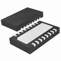
LTC4217CDHC#PBF Linear Technology, LTC4217CDHC#PBF Datasheet - Page 4

LTC4217CDHC#PBF
Manufacturer Part Number
LTC4217CDHC#PBF
Description
IC CTRLR HOT SWAP 2A 16-DFN
Manufacturer
Linear Technology
Type
Hot-Swap Switchr
Datasheet
1.LTC4217IFEPBF.pdf
(18 pages)
Specifications of LTC4217CDHC#PBF
Applications
General Purpose
Internal Switch(s)
Yes
Current Limit
2.0A
Voltage - Supply
2.9 V ~ 26.5 V
Operating Temperature
0°C ~ 70°C
Mounting Type
Surface Mount
Package / Case
16-WFDFN Exposed Pad
Linear Misc Type
Positive Low Voltage
Package Type
DFN EP
Operating Supply Voltage (min)
2.9V
Operating Temperature (min)
0C
Operating Temperature (max)
70C
Operating Temperature Classification
Commercial
Product Depth (mm)
3mm
Product Length (mm)
5mm
Mounting
Surface Mount
Pin Count
16
Lead Free Status / RoHS Status
Lead free / RoHS Compliant
Available stocks
Company
Part Number
Manufacturer
Quantity
Price
ELECTRICAL CHARACTERISTICS
LTC4217
temperature range, otherwise specifications are at T
SYMBOL
Inputs
I
R
V
∆V
∆V
V
∆V
R
Outputs
V
I
V
V
I
I
I
A
I
I
I
I
AC Characteristics
t
t
t
t
t
Note 1: Stresses beyond those listed under Absolute Maximum Ratings
may cause permanent damage to the device. Exposure to any Absolute
Maximum Rating condition for extended periods may affect device
reliability and lifetime.
Note 2: All currents into pins are positive, all voltages are referenced to
GND unless otherwise specified.
Note 3: An internal clamp limits the GATE pin to a maximum of 6.5V above
OUT. Driving this pin to voltages beyond the clamp may damage the device.
Note 4: This IC includes overtemperature protection that is intended
to protect the device during momentary overload conditions. Junction
4
IN
OH
TIMER(UP)
TIMER(DN)
TIMER(RATIO)
OFF(IMON)
GATE(UP)
GATE(DN)
GATE(FST)
PHL(GATE)
PHL(ILIM)
D(ON)
D(CB)
D(AUTO-RETRY)
TH
UV(RTH)
OL
TIMER(H)
TIMER(L)
IMON
IN
ISET
OV(HYST)
UV(HYST)
FB(HYST)
PARAMETER
OV, UV, FB Pin Input Current
OV, UV, FB Pin Input Resistance
OV, UV, FB Pin Threshold Voltage
OV Pin Hysteresis
UV Pin Hysteresis
UV Pin Reset Threshold Voltage
FB Pin Power Good Hysteresis
I
PG, FLT Pin Output Low Voltage
PG, FLT Pin Input Leakage Current
TIMER Pin High Threshold
TIMER Pin Low Threshold
TIMER Pin Pull-Up Current
TIMER Pin Pull-Down Current
TIMER Pin Current Ratio I
I
I
Gate Pull-Up Current
Gate Pull-Down Current
Gate Fast Pull-Down Current
Input High (OV), Input Low (UV) to Gate Low
Propagation Delay
Short-Circuit to Gate Low
Turn-On Delay
Circuit Breaker Filter Delay Time (Internal)
Auto-Retry Turn-On Delay (Internal)
SET
MON
MON
Pin Output Resistor
Pin Current Gain
Pin Offset Current
TIMER(DN)
/I
TIMER(UP)
A
= 25°C. V
CONDITIONS
V
LTC4217-12
V
V
C-Grade, I-Grade
H-Grade
I
V
V
V
V
V
I
I
Gate Drive On, V
Gate Drive Off, V
Fast Turn Off, V
V
V
Step V
V
OUT
OUT
OUT
V
IN
IN
UV
OUT
TIMER
TIMER
TIMER
TIMER
FB
GATE
FB
GATE
C-Grade, I-Grade
H-Grade
C-Grade, I-Grade
H-Grade
C-Grade, I-Grade
H-Grade
The
= 1.2V, LTC4217
Rising
= 0, Step I
= 0V, Step I
Falling
= 2mA
= 2A
= 132mA
= 30V
< 16.5V Falling
UV
< 16.5V Falling
Rising
Falling
= 0V
= 1.2V
l
DD
to 2V, V
denotes the specifications which apply over the full operating
= 12V unless otherwise noted.
SENSE
SENSE
GATE
temperature will exceed 125°C when overtemperature protection is active.
Continuous operation above the specified maximum operating junction
temperature may impair device reliability.
Note 5: T
dissipation, P
Note 6: For the DHC package, switch on-resistance is guaranteed by
design and test correlation.
GATE
GATE
GATE
LTC4217DHC, LTC4217DHC-12: T
LTC4217FE: T
= 18V, V
to 1.2A,
= V
= 18V, V
to 1.2A
> 13V
OUT
J
is calculated from the ambient temperature, T
OUT
= 12V
OUT
D
, according to the formula:
= 12V
J
= 12V
= T
A
+ (P
D
l
l
l
l
l
l
l
l
l
l
l
l
l
l
l
l
l
l
l
l
l
l
l
l
l
l
l
l
• 38°C/W)
1.21
0.55
19.5
19.2
47.5
MIN
–80
–19
190
164
1.2
0.1
1.4
1.6
1.5
1.4
J
13
10
50
10
50
50
= T
A
+ (P
1.235
1.235
–100
0.62
0.21
TYP
–24
250
140
140
100
100
0.4
0.4
D
18
20
80
20
20
20
50
0
0
2
2
0
8
1
2
2
• 43°C/W)
A
–120
, and power
MAX
1.26
20.5
20.8
0.92
1.28
52.5
±7.5
110
±10
–29
340
355
150
150
0.7
0.8
0.3
2.6
2.7
2.7
2.7
±1
23
30
30
10
5
UNITS
4217fd
µA/A
mV
mV
mV
mA
ms
ms
ms
ms
kΩ
kΩ
kΩ
µA
µA
µA
µA
µA
µA
µA
µA
µs
µs
%
V
V
V
V
V
V


