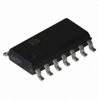
MIC2595-2BM Micrel Inc, MIC2595-2BM Datasheet - Page 16

MIC2595-2BM
Manufacturer Part Number
MIC2595-2BM
Description
IC CTRLR HOT SWAP NEG HV 14-SOIC
Manufacturer
Micrel Inc
Type
Hot-Swap Controllerr
Datasheet
1.MIC2589R-1YM_TR.pdf
(29 pages)
Specifications of MIC2595-2BM
Applications
General Purpose
Internal Switch(s)
No
Voltage - Supply
-19 V ~ -80 V
Operating Temperature
-40°C ~ 85°C
Mounting Type
Surface Mount
Package / Case
14-SOIC (0.154", 3.90mm Width)
Lead Free Status / RoHS Status
Contains lead / RoHS non-compliant
Available stocks
Company
Part Number
Manufacturer
Quantity
Price
Company:
Part Number:
MIC2595-2BM
Manufacturer:
MICREL
Quantity:
4 197
December 2005
Functional Description
Hot Swap Insertion
When circuit boards are inserted into systems carrying
live supply voltages (“hot swapped”), high inrush
currents often result due to the charging of bulk
capacitance that resides across the circuit board’s
supply pins. These current spikes can cause the
system’s supply voltages to temporarily go out of
regulation causing data loss or system lock-up. In
more extreme cases, the transients occurring during a
hot swap event may cause permanent damage to
connectors or onboard components.
The MIC2589 and the MIC2595 are designed to
address these issues by limiting the maximum current
that is allowed to flow during hot swap events. This is
achieved by implementing a constant-current loop at
turn-on. In addition to inrush current control, the
MIC2589 and the MIC2595 incorporate input voltage
supervisory
overcurrent protection,
protection for both the system and the circuit board.
GATE Start-Up and Control
When the input voltage to the controller is between
the overvoltage and undervoltage threshold settings
(MIC2589) or is greater than the ON threshold setting
(MIC2595), a start cycle is initiated to deliver power to
the load. During the start-up cycle, the GATE pin of
the controller applies a constant charging current
(45µA, nominal) to the gate of the external MOSFET,
charging the MOSFET gate from 0V to 10V,
referenced to V
used to adjust and control the slew rate of the GATE
output, while resistor R4 can be used to minimize the
potential for parasitic high-frequency oscillations
occurring on the gate of the external MOSFET (M1).
See Typical Application circuit.
equation is used to approximate the expected inrush
current given the values of the capacitance at the gate
and the load (i.e., the gate of the external MOSFET
and the drain of the external MOSFET, respectively).
Active current limiting for the MIC2589/MIC2595 is
implemented by controlling the voltage on the GATE
pin
MIC2589/MIC2595 is defined to be in current limit
when the GATE output voltage level is between 2.5V
and 5.5V.
voltage is regulated to limit the load current to the
programmed
via
an
INRUSH
Once in current limit, the GATE output
functions
EE
value
internal
. An external capacitor (C2) can be
=
C
C
(I
LOAD
GATE
LIMIT
and
thereby
feedback
).
×
I
user
GATE(ON)
Additionally,
providing robust
circuit.
The following
programmable
The
the
16
overcurrent delay and the no-load detection timers
must be set accordingly to allow the output load to
fully charge during the start-up cycle. See the “Circuit
Breaker Function” and “No-Load Detection” sections
for further details.
Resistor R4, in series with the power MOSFET’s gate,
may be required in some layouts to minimize the
potential for parasitic oscillations occurring in M1.
Note that resistance in this device of the circuit has a
slight
MIC2589/MIC2595’s
possible, use high-frequency PCB layout techniques
and use a dummy resistor (R4 = 0Ω) for the initial
evaluation. If during prototyping an R4 is required,
common values for R4 range between 4.7Ω to 20Ω for
various power MOSFETs.
Circuit Breaker Function
The MIC2589 and MIC2595 device family employs an
electronic circuit breaker that protects the external
power MOSFET and other system components
against large-scale faults, such as short circuits. The
current-limit threshold is set via an external resistor,
R
An overcurrent filter period is set via a capacitor from
the CFILTER pin to ground (C
the length of the time period (t
remains in current limit before the circuit breaker is
tripped. This programmable delay prevents tripping of
the circuit breaker due to the large inrush current
charging bulk and distributed capacitive loads.
Whenever the voltage across R
two things happen:
SENSE
1. A constant-current regulation loop is engaged
2. Capacitor C
, connected between the VEE and SENSE pins.
which is designed to hold the voltage across
R
load and the MIC2589/MIC2595 circuits from
excessively
regulation loop will engage in less than 1µs
from the time at which the overcurrent trip
threshold on R
V
I
source. If the voltage across CFILTER
crosses this threshold, the circuit breaker trips
and the GATE pin is immediately pulled low
by
operation turns off the MOSFET quickly and
disconnects the input from the load. The time
period that allows for the output to regulate in
CFILTER(CHARGE)
CFILTER(TRIP)
SENSE
destabilizing
an
equal to 50mV. This protects both the
internal
I
LIMIT
FILTER
high
SENSE
current
threshold
an
=
is charged up to an internal
R
current
V
is exceeded.
currents.
SENSE
effect
internal
TRIP
FLT
FILTER
SENSE
) for which the device
regulation
) that determines
of
pull-down.
exceeds 50mV,
95µA
This
(408) 955-1690
upon
M9999-120505
1.25V
loop.
current-
current
This
the
by
If


