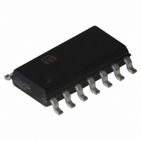
MIC2595-2BM Micrel Inc, MIC2595-2BM Datasheet - Page 18

MIC2595-2BM
Manufacturer Part Number
MIC2595-2BM
Description
IC CTRLR HOT SWAP NEG HV 14-SOIC
Manufacturer
Micrel Inc
Type
Hot-Swap Controllerr
Datasheet
1.MIC2589R-1YM_TR.pdf
(29 pages)
Specifications of MIC2595-2BM
Applications
General Purpose
Internal Switch(s)
No
Voltage - Supply
-19 V ~ -80 V
Operating Temperature
-40°C ~ 85°C
Mounting Type
Surface Mount
Package / Case
14-SOIC (0.154", 3.90mm Width)
Lead Free Status / RoHS Status
Contains lead / RoHS non-compliant
Available stocks
Company
Part Number
Manufacturer
Quantity
Price
Company:
Part Number:
MIC2595-2BM
Manufacturer:
MICREL
Quantity:
4 197
December 2005
where V
C
VEE. Once the voltage on CNLD reaches its no-load
threshold voltage, V
controller will shut down until it is reset manually
(MIC2589/MIC2595) or until it performs an auto-retry
operation (MIC2589R/MIC2595R). During start-up, the
no-load detection circuit begins to monitor the load
current and the CNLD pin starts ramping along with
the GATE output. In order to keep the output from
shutting down, t
that the output MOSFET switches on to deliver the
required minimum load-detect current to the output
load before the no-load timer times out.
The Power-Good Output Signals
For
MIC2589R/MIC2595R-1, power-good output signal
PWRGD1 will be high impedance when V
below V
DRAIN when V
MIC2589/95-2 and the MIC2589R/95R-2, power-good
output signal /PWRGD1 will pull down to the potential
of the DRAIN pin when V
will be high impedance when V
Hence, the -1 parts have an active-high PWRGDX
signal and the -2 parts have an active-low /PWRGDX
output. PWRGDX (or /PWRGDX) may be used as an
enable signal for one or more following DC/DC
converter modules or for other system uses as
desired. When used as an enable signal, the time
necessary for the PWRGD (or /PWRGD) signal to
pull-up (when in high impedance state) will depend
upon the load (RC) that is present on this output.
Power-good output signals PWRGD2 (/PWRGD2) and
PWRGD3
PWRGD1 (/PWRGD1) with a sequencing delay set by
an external capacitor (C
PGTIMER pin (Pin 2) to VEE. An expression for the
sequencing delay between PWRGD2 and PWRGD1
is given by:
where VTHRESH(PG2) (= 0.63V, typically) is the
PWRGD2 threshold voltage for PGTIMER and I
(= 45µA, typically) is the internal PGTIMER charge
current. Similarly, an expression for the sequencing
delay between PWRGD3 and PWRGD2 is given by:
t
NLD
NLD
t
PGDLY2
is an external capacitor connected from Pin 6 to
=
V
PGTH
CNLD
CNLD
−
the
1
, and will pull-down to the potential at the
(/PWRGD3)
=
= 1.24V (typ); I
×
V
⎛
⎜
⎜
⎝
NLD
THRESH(PG2
I
C
DRAIN
CNLD
NLD
CNLD
must be long enough to ensure
I
PGTIMER
MIC2589/MIC2595-1
⎞
⎟
⎟
⎠
, the loop times out and the
is above V
DRAIN
follow
PG
)
) from the controller’s
×
CNLD
drops below V
C
DRAIN
PG
the
= 25µA (typ); and
is above V
PGTH
assertion
. For the
DRAIN
PGTH
PGTIMER
drops
PGTH
and
and
of
.
18
where V
threshold voltage for PGTIMER. Therefore, power-
good output signal PWRGD2 (/PWRGD2) will be
delayed after the assertion of PWRGD1 (/PWRGD1)
by:
t
Power-good output signal PWRGD3 (/PWRGD3)
follows the assertion of PWRGD2 by a delay:
t
For example, for a 10µF value for C
output signal PWRGD2 will be asserted 140ms after
PWRGD1. Power-good signal PWRGD3 will then be
asserted 115ms after PWRGD2 and 255ms after the
assertion of PWRGD1. The relationships between
V
are shown in Figure 6.
Undervoltage/Overvoltage Detection (MIC2589 and
MIC2589R)
The MIC2589 and the MIC2589R have “UV” and “OV”
input pins that can be used to detect input supply rail
undervoltage
Undervoltage lockout prevents the output from
switching on until the supply input is stable and within
tolerance. In a similar fashion, overvoltage shutdown
prevents damage to sensitive circuit components
should the input voltage exceed normal operating
limits. Each of these pins is internally connected to
analog comparators with 20mV of hysteresis. When
the UV pin falls below its V
is above its V
immediately pulled low. The GATE pin will be held low
until the UV pin is above its V
pin is below its V
OV threshold voltage levels are programmed using
the resistor divider R1, R2, and R3 as shown in the
“Typical Application” circuit and the equations to set
the trip points are shown below. The circuit’s UV
threshold is set to V
set at V
Office power distribution applications.
Given V
the remaining two resistor values can be determined.
A suggested value for R3 is selected to provide
approximately 100µA (or more) of current through the
voltage divider chain at V
t
V
V
PGDLY2-1
PGDLY3-2
PGDLY3
DRAIN
UV
OV
=
=
, V
V
V
−
(ms) ≅ 14 × C
(ms) ≅ 11.5 × C
OV
UV
THRESH(PG3)
UVL
OVL
2
PGTH
, V
=
= 72V, values commonly used in Central
(typ)
(
(typ)
V
, PWRGD1, PWRGD2, and PWRGD3
OV
THRESH(PG3
, and any one of the resistor values,
OVH
×
×
and
OVL
(
(
(1.15V, typical) is the PWRGD3
R1
UV
R1
(
threshold. The circuit’s UV and
PG
R2
threshold, the GATE pin is
= 37V and the OV threshold is
+
+
PG
(µF)
R2
R2
R3
+
(µF)
)
overvoltage
UVL
I
R3
DD
PGTIMER
−
+
+
UVH
V
R3
R3
)
threshold or the OV pin
= V
THRESH(PG2
)
threshold and the OV
)
UV
. This yields the
PG
(408) 955-1690
M9999-120505
, power-good
)
conditions.
)
×
C
PG


