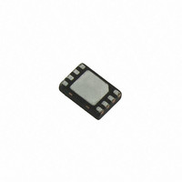
LDS8681008-T2 IXYS, LDS8681008-T2 Datasheet

LDS8681008-T2
Specifications of LDS8681008-T2
LDS8681-002-T6-2
LDS8681-002-T6-2
LDS8681008-T2-2
Related parts for LDS8681008-T2
LDS8681008-T2 Summary of contents
Page 1
... The LDS8681 is a high efficiency regulated charge pump with low dropout voltage that can drive two TYPICAL APPLICATION CIRCUIT © 2009 IXYS Corp. Characteristics subject to change without notice LEDs at 400 mA each simultaneously or one LED at 800 mA. Low dropout PowerLite™ Current Regulator (PCR) increases device’ ...
Page 2
... Flash LED Turn-on Time 2-x mode 3 PWM Frequency Note: 1. Sample test only 2. Measusured from EN LOW to HIGH transition See Current setting Error vs. Duty Cycle and PWM Frequency at p.3 © 2009 IXYS Corp. Characteristics subject to change without notice Rating Unit 0.7V ...
Page 3
... Ch3 – Output voltage Operating Waveforms at 1kHz PWM mode 10% Duty Cycle V = 4.2 V, Ch1 – PWM, Ch2 – LED current (400 mA/div) IN LED Current Setting Error vs. Duty Cycle © 2009 IXYS Corp. Characteristics subject to change without notice = 2 μ C1= 1μ 25°C unless otherwise specified IN OUT ...
Page 4
... OUT the LED anodes. A small 2.2 μ F ceramic bypass capacitor is required between the V ground near the device. © 2009 IXYS Corp. Characteristics subject to change without notice Function GND is the ground reference for the charge pump. The pin must be connected to the ground plane on the PCB ...
Page 5
... LED forward voltage V significantly increasing F © 2009 IXYS Corp. Characteristics subject to change without notice driver’s efficiency. The LDS8681 monitors voltage drop Vd across PCR at every channel in ON state. If this voltage falls below 150 mV (typical) at any one ...
Page 6
... If the power source is a Li-ion battery, LEDs with lowest forward voltages are recommended to achieve highest efficiency and extended operation on a single battery charge. © 2009 IXYS Corp. Characteristics subject to change without notice LEDs with forward voltages ( may be used. Charge pump operates in highest efficiency when V multiplied by switching mode, i ...
Page 7
... E 1.950 2.000 E1 1.550 1.600 e 0.500 Bsc L 0.350 0.400 Note: 1. All dimensions are in millimeters 2. Complies with JEDEC Standard MO-220 © 2009 IXYS Corp. Characteristics subject to change without notice MAX 0.800 0.050 0.280 3.050 1.850 2.050 1.650 0.450 7 Doc. No. 8681_DS, Rev. N1.0 ...
Page 8
... The standard lead finish is Matte-Tin. 3) The device used in the above example is a LDS8681 008–T2 (2x3 TDFN, Tape & Reel). 4) For additional package and temperature options, please contact your nearest IXYS Corp. Sales office. © 2009 IXYS Corp. Characteristics subject to change without notice Package ...
Page 9
... IXYS Corp. products are not designed, intended, or authorized for use as components in systems intended for surgical implant into the body, or other applications intended to support or sustain life, or for any other application in which the failure of the IXYS Corp. product could create a situation where personal injury or death may occur. ...


