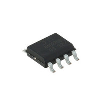
ZXLD1366EN8TC Diodes Zetex, ZXLD1366EN8TC Datasheet - Page 18

ZXLD1366EN8TC
Manufacturer Part Number
ZXLD1366EN8TC
Description
SEMICONDUCTOR OTHER
Manufacturer
Diodes Zetex
Datasheet
1.ZXLD1366ET5TA.pdf
(30 pages)
Specifications of ZXLD1366EN8TC
Constant Current
*
Constant Voltage
*
Topology
*
Number Of Outputs
*
Internal Driver
*
Type - Primary
*
Type - Secondary
*
Frequency
*
Voltage - Supply
*
Voltage - Output
*
Mounting Type
Surface Mount
Package / Case
8-SOIC (0.154", 3.90mm Width) Exposed Pad
Operating Temperature
*
Current - Output / Channel
*
Lead Free Status / RoHS Status
Lead free / RoHS Compliant
Other names
ZXLD1366EN8TCTR
Available stocks
Company
Part Number
Manufacturer
Quantity
Price
Company:
Part Number:
ZXLD1366EN8TC
Manufacturer:
Diptronics
Quantity:
60 000
Part Number:
ZXLD1366EN8TC
Manufacturer:
ZETEX
Quantity:
20 000
Application Information
Setting nominal average output current with external resistor R
The nominal average output current in the LED(s) is determined by the value of the external current sense resistor (R
connected between VIN and ISENSE and is given by:
I
The table below gives values of nominal average output current for several preferred values of current setting resistor (R
the typical application circuit shown on page 1:
The above values assume that the ADJ pin is floating and at a nominal voltage of V
minimum allowed value of sense resistor under these conditions to maintain switch current below the specified maximum
value.
It is possible to use different values of R
Output current adjustment by external DC control voltage
The ADJ pin can be driven by an external dc voltage (V
the nominal average value defined by R
The nominal average output current in this case is given by:
I
Note that 100% brightness setting corresponds to
increased in proportion to prevent I
The input impedance of the ADJ pin is 50kΩ ±25% for voltages below V
+100mV.
Output current adjustment by PWM control
Directly driving ADJ input
A Pulse Width Modulated (PWM) signal with duty cycle DPWM can be applied to the ADJ pin, as shown below, to adjust the
output current to a value above or below the nominal average value set by resistor R
ZXLD1366
Document number: DS31992 Rev. 6 - 2
DC
OUTnom
OUTdc
R
0.20
0.27
0.56
S
GND
+
(Ω)
= (V
= 0.2/R
ADJ
S
Nominal average output
/1.25) x (0.2/R
for R
ADJ
current (mA)
S
≥ 0.2Ω
1000
740
357
ZXLD1366
S
) for 0.3< V
OUTdc
GND
S
S
.
exceeding 1A maximum.
if the ADJ pin is driven from an external voltage. (See next section).
ADJ
<2.5V
www.diodes.com
V
ADJ
ADJ
), as shown, to adjust the output current to a value above or below
18 of 30
= V
REF
. When driving the ADJ pin above 1.25V, R
S
REF
and 14.2kΩ ±25% for voltages above V
Diodes Incorporated
A Product Line of
S
REF
:
(=1.25V). Note that R
© Diodes Incorporated
ZXLD1366
S
March 2011
= 0.2Ω is the
S
must be
REF
S
) in
S
)


