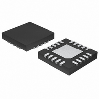
MAX8790AETP+T Maxim Integrated Products, MAX8790AETP+T Datasheet - Page 19

MAX8790AETP+T
Manufacturer Part Number
MAX8790AETP+T
Description
IC LED DRVR WHITE BCKLGT 20-TQFN
Manufacturer
Maxim Integrated Products
Type
Backlight, White LEDr
Datasheet
1.MAX8790AETP.pdf
(23 pages)
Specifications of MAX8790AETP+T
Topology
PWM, Step-Up (Boost)
Number Of Outputs
6
Internal Driver
No
Type - Primary
Backlight
Type - Secondary
White LED
Frequency
1MHz
Voltage - Supply
4.5 V ~ 5.5 V, 5.5 V ~ 26 V
Voltage - Output
5V
Mounting Type
Surface Mount
Package / Case
20-TQFN Exposed Pad
Operating Temperature
-40°C ~ 85°C
Current - Output / Channel
27mA
Internal Switch(s)
Yes
Lead Free Status / RoHS Status
Lead free / RoHS Compliant
Efficiency
-
Lead Free Status / Rohs Status
Details
The total output voltage ripple has two components: the
capacitive ripple caused by the charging and discharging
on the output capacitor, and the ohmic ripple due to the
capacitor’s equivalent series resistance (ESR):
and:
where I
Inductor Selection section ).
The output voltage-ripple voltage should be low
enough for the FB_ current-source regulation. The rip-
ple voltage should be less than 200mV
capacitors, the output-voltage ripple is typically domi-
nated by V
ture characteristics of the output capacitor must also
be considered.
The MAX8790A’s step-up converter uses an external
MOSFET to enable applications with scalable output
voltage and output power. The boost switching architec-
ture is simple and ensures that the controller is never
exposed to high voltage. Only the external MOSFET,
diode, and inductor are exposed to the output voltage
plus one Schottky diode forward voltage:
The MOSFET’s breakdown ratings should be higher
than V
bility. A conservative rule of thumb, a minimum 30%
margin would be recommended for MOSFET break-
down voltage. The external MOSFET should have a cur-
rent rating of no less than the I
Inductor Selection section. To improve efficiency,
choose a MOSFET with low R
gate-drive linear regulator can provide 10mA. Select the
external MOSFET with a total gate charge so the aver-
age current to drive the MOSFET at maximum switching
frequency is less than 10mA:
For example, the Si3458DV is specified with 16nC of
max total gate charge at Vg = 10V. For 5V of gate
drive, the required gate charge is 8nC, which equates
to 8mA at 1MHz.
V
Current Balancing for LCD Panel Applications
RIPPLE C
BV
PEAK
V
with sufficient margin to ensure long-term relia-
BV
V
RIPPLE(C)
RIPPLE
( )
V
= ×
RIPPLE ESR
N V
is the peak inductor current (see the
≈
Q
I
OUT MAX
g MAX
______________________________________________________________________________________
F LED
=
C
(
(
External MOSFET Selection
_
Output Capacitor Selection
Six-String White LED Driver with Active
V
OUT
. The voltage rating and tempera-
(
RIPPLE C
)
)
×
≈
+
)
I
f
V
PEAK ESR COUT
OSC
⎛
⎜
⎝
( )
F SCHOTTKY
V
_
OUT MAX
DS(ON)
+
V
<10
R
PEAK
OUT MAX OSC
V
(
RIPPLE ESR
mA
(
. The MAX8790A’s
(
derived from the
)
P-P
−
(
)
+
V
f
. For ceramic
IN MIN
V
)
FB
(
)
_
)
⎞
⎟
⎠
The MOSFET conduction loss or resistive loss is
caused by the MOSFET’s on-resistance (R
power loss can be estimated as:
For the above Si3458DV, the estimated conduction loss is:
The approximate maximum switching loss can be cal-
culated as:
For the above Si3458DV, the approximate switching
loss is:
The MAX8790A’s high switching frequency demands a
high-speed rectifier. Schottky diodes are recommended
for most applications because of their fast recovery
time and low forward voltage. The diode should be
rated to handle the output voltage and the peak switch
current. Make sure that the diode’s peak current rating
is at least I
section and that its breakdown voltage exceeds the
output voltage.
The OV protection circuit should ensure the circuit safe
operation; therefore, the controller should limit the out-
put voltage within the ratings of all MOSFET, diode, and
output capacitor components, while providing sufficient
output voltage for LED current regulation. The OV pin is
connected to the center tap of a resistive voltage-
divider (R1 and R2 in Figure 1) from the high-voltage
output. When the controller detects the OV pin voltage
reaching the threshold V
tection is activated. Hence, the step-up converter out-
put overvoltage protection point is:
In Figure 1, the output OVP voltage is set to:
PD
PD
Setting the Overvoltage Protection Limit
SW MAX
RES MAX
PD
(
PD
(
V
SW MAX
OUT OVP
RES MAX
)
PEAK
(
)
=
V
=
(
(
OUT OVP
10
0 1
.
)
ns
calculated in the Inductor Selection
=
)
Ω
(
)
=
×
=
t
×
turn off
1 23
1 35
R
4 7
.
.
)
DS ON
.
Rectifier Diode Selection
=
−
OV_TH
μ ×
V
A
(
V
H
× +
OV TH
×
3 7
×
(
28 72
1
)
2
×
3
750
I
_
PEAK
× ×
, typically 1.23V, OV pro-
×
.
L f
V
37 4
V
1
kHz
IN MIN
2
× +
V
M
.
OSC
×
(
(
×
1
Ω
k
V
×
Ω
750
OUT
1 35
R
R
)
)
.
×
1
2
=
kHz
I
PEAK
)
34 1
DS(ON)
A
×
3
f
.
OSC
=
V
=
3
0 145
0 04
.
). This
.
W
19
W


