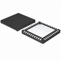
MAX6974ATL+ Maxim Integrated Products, MAX6974ATL+ Datasheet - Page 2

MAX6974ATL+
Manufacturer Part Number
MAX6974ATL+
Description
IC LED DRIVER LINEAR 40-TQFN
Manufacturer
Maxim Integrated Products
Type
Linear (Serial Interface)r
Datasheet
1.MAX6975ATL.pdf
(23 pages)
Specifications of MAX6974ATL+
Topology
PWM
Number Of Outputs
24
Internal Driver
Yes
Type - Primary
General Purpose
Type - Secondary
RGB
Frequency
33MHz
Voltage - Supply
3 V ~ 3.6 V
Voltage - Output
7V
Mounting Type
Surface Mount
Package / Case
40-TQFN Exposed Pad
Operating Temperature
-40°C ~ 125°C
Current - Output / Channel
30mA
Internal Switch(s)
Yes
Low Level Output Current
6 mA
High Level Output Current
30 mA
Operating Supply Voltage
3 V to 3.6 V
Maximum Supply Current
77 mA
Maximum Power Dissipation
2963 mW
Maximum Operating Temperature
+ 125 C
Mounting Style
SMD/SMT
Minimum Operating Temperature
- 40 C
Lead Free Status / RoHS Status
Lead free / RoHS Compliant
Efficiency
-
Lead Free Status / Rohs Status
Lead free / RoHS Compliant
ABSOLUTE MAXIMUM RATINGS
(All voltages with respect to GND.)
V
R0–R7, G0–G7, B0–B7, MUX0, and MUX1 ...........-0.3V to +8.0V
All Other Pins..............................................-0.3V to (V
Continuous Power Dissipation (T
24-Output PWM LED Drivers
for Message Boards
Stresses beyond those listed under “Absolute Maximum Ratings” may cause permanent damage to the device. These are stress ratings only, and functional
operation of the device at these or any other conditions beyond those indicated in the operational sections of the specifications is not implied. Exposure to
absolute maximum rating conditions for extended periods may affect device reliability.
ELECTRICAL CHARACTERISTICS
(V
2
Operating Supply Voltage
LEDs Anode Voltage
(R0–R7, G0–G7, B0–B7, MUX0,
and MUX1)
Supply Current
Input High Voltage LOADI
Input Low Voltage LOADI
Differential Input Voltage Range
CLKI_, DIN_
Common-Mode Input Voltage
CLKI_, DIN_
Differential Input High Threshold
Differential Input Low Threshold
Differential Output Voltage
CLKO_, DOUT_
Differential Output Offset
CLKO_, DOUT_
Input Leakage Current
CLKI_, DIN_, LOADI
Input Capacitance
CLKI_, DIN_, LOADI
Output Low Voltage LOADO
Output High Voltage LOADO
DD
DD
40-Pin TQFN (derate 37mW/°C over +70°C) .............2963mW
_______________________________________________________________________________________
........................................................................-0.3V to +4.0V
= 3.0V to 3.6V, T
PARAMETER
A
= T
MIN
to T
A
= +70°C)
MAX
SYMBOL
VDIFF
VDIFF
, unless otherwise noted. Typical values are at V
I
V
V
V
IH
V
V
V
V
V
I
V
V
OHC
OLC
DD
IHC
ILC
CM
DD
OD
OS
, I
ID
O
IL
TH
TL
f
calibration DACs set to 0x01
f
calibration DACs set to 0xFF
f
calibration DACs set to 0xFF
Termination 200Ω at receiver _+ and _- inputs
Termination 200Ω at receiver _+ and _- inputs
I
I
CLKI
CLKI
CLKI
SINK
SOURCE
DD
= 0Hz; CLKO_, DOUT_ loaded 200Ω;
= 0Hz; CLKO_, DOUT_ loaded 200Ω;
= 32MHz; CLKO_, DOUT_ loaded 200Ω;
= 5mA
+ 0.3V)
= 5mA
CONDITIONS
Operating Temperature Range .........................-40°C to +125°C
Junction Temperature ......................................................+150°C
Storage Temperature Range .............................-65°C to +150°C
Lead Temperature (soldering, 10s) .................................+300°C
DD
= 3.3V, T
A
| V
V
- 0.5
x V
±0.15
1.125
±190
= +85°C.) (Note 1)
-100
MIN
I D
DD
3.0
0.7
-1
DD
/ 2|
- 0.2
TYP
1.25
0.05
V
28
51
54
10
-8
8
DD
x V
±1.20
1.375
±550
MAX
0.25
100
3.6
0.3
2.4
+1
52
72
77
7
DD
UNITS
mA
mV
mV
mV
µA
pF
V
V
V
V
V
V
V
V
V


