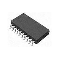
NJU6051V-TE1 NJR, NJU6051V-TE1 Datasheet

NJU6051V-TE1
Specifications of NJU6051V-TE1
Related parts for NJU6051V-TE1
NJU6051V-TE1 Summary of contents
Page 1
... Built-in Temperature Compensation Circuit to Suppress the Characteristic Degradation of LEDs # Uses Small Inductor and Capacitors # 1.8V to 3.6V Operating Voltage for Logic Circuits (V # 3.0V to 5.5V Operating Voltage for Step-up Circuits (V # CMOS Technology # Package : QFN20 / SSOP20 Ver.2003-10-23 = 30mA ) DDL ) DD NJU6051 PRELIMINARY ! PACKAGE OUTLINE NJU6051KM1 NJU6051V - 1 - ...
Page 2
NJU6051 ! QFN20 PIN CONNECTIONS (TOP VIEW) FB VOUT SSOP20 PIN CONNECTIONS (TOP VIEW TEST NC VDD VDDL REQ DATA SCK - 2 - VSO SENS RSTb SCK DATA VOUT FB VSS VSS ...
Page 3
PIN DESCRIPTION No. SYMBOL QFN SSOP DDL SCK 6 9 DATA 1 4 TEST 5 8 REQ 9 12 SENS 8 11 RSTb ...
Page 4
NJU6051 ! BLOCK DIAGRAM V SO Regulator SENS C1 A/D Converter Register V DDL Serial REQ Interface SCK DATA Reset RSTb CX/TCLK OSC - PWM Controller OUT A1 FB Logic REF ...
Page 5
FUNCTIONAL DESCRIPTONS (1) LED CURRENT CONTROL The NJU6051 incorporates the LED current control circuit to regulate the LED current (I programmed by the feedback resistor ( internally regulated to 0.6V typical and connected to the positive input ...
Page 6
NJU6051 (4) PWM DIMMING CONTROL By setting the duty data at “PWM REGISTER” bits, 8 out of 64 registers are assigned to the PWM REGISTER 0-7. The PWM duty is changed depending on the register selected by the SENS voltage. ...
Page 7
SERIAL INTERFACE (5-1) SERIAL DATA WRITE The serial data is latched into the shift register on the rising edge of the serial clock (SCK), and determined on the rising edge of the data request (REQ). The serial data format ...
Page 8
NJU6051 (5-2) SENSOR DATA READ The DATA terminal becomes output state by setting the REQ terminal to “1” after the command data transmission. And the sensor data is read out, synchronizing with the SCK. The bit number corresponding to a ...
Page 9
HOLD By setting “1” at the HOLD bit, the selected PWM REGISTER is held and the luminance sensor control cannot be used. In other words, this setting works so that the luminance of the LEDs doesn’t change even if ...
Page 10
NJU6051 And, the formula (3) gives the PWM frequency osc f pwm TABLE 7 PWM FREQUENCY DIVIDE NOTE) PWM frequencies written in bold ...
Page 11
APPLICATIONS INFORMATION (9-1) PWM DUTY and LED CURRENT The average LED current is programmed with the single resistor R Formula (4). DUTY I I LED(avg) LED(max) 100 V REF I LED(max) R LED (9-2) INDUCTOR SELECTION Formula (5) is ...
Page 12
NJU6051 ! ABSOLUTE MAXIMUM RATINGS PARAMETERS SYMBOL VDD Power Supply V VDDL Power Supply V Input Voltage V Input Voltage V Switch Voltage V Power Dissipation PD Operating Temperature T Storage Temperature T NOTE1) All voltages are relative to V ...
Page 13
DC ELECTRICAL CHARACTERISTICS PARAMETERS SYMBOL V Power Supply Power Supply V DDL Output Current I OUT Reference Voltage V Operating Current I OPR Standby Current I STBY V Power Supply V SO PWM REGISTER0 V Selected ...
Page 14
NJU6051 NOTE1) Output Voltage Test Conditions ! TEST Command TEST Circuit LED :V =3.6V VDD :5V D1 :Schottky diode L1 :6.8uH C1 :4.7uF C2 :1uF R1 :100k RLED :40 fOSC :500kHz ...
Page 15
NOTE2) TEMPERATURE COMPENSATION The reference voltage (V ) generator has temperature compensation, which suppresses the characteristic-degradation of REF LEDs at high temperatures. The V REF as the ambient temperature rises in the range higher than 45°C. 1.0 0.5 0.0 -50 ...
Page 16
NJU6051 NOTE3) Operating Current Test Conditions ! TEST Command NOTE4) Standby Current ! TEST Command TEST Circuit (Operating Current, Standby Ciurrent) LED :V =3.6V ...
Page 17
NOTE5) V Power Supply Test Condition SO ! TEST Command TEST Circuit LED :V =3.6V :Schottky diode L1 :6.8uH C1 :4.7uF C2 :1uF R1 :100K R2 :1K R :40 LED ...
Page 18
NJU6051 NOTE6) OSCILLATOR The built-in oscillator incorporates a reference power supply, so its frequency is independent from the V is varied by the external capacitor CX, as shown below fOSC vs CX 1000 900 800 700 600 ...
Page 19
AC ELECTRICAL CHARACTERISTICS PARAMETERS SCK Clock Cycle “H” Level SCK Clock Width “L” Level REQ Hold Time Data Set-Up Time Data Hold Time Output Data Delay Time CL=20pF REQ Set-Up Time REQ High Level Width REQ,SCK,DATA Rising Time REQ,SCK,DATA ...
Page 20
NJU6051 ! TYPICAL APPLICATION CIRCUIT SENS V DDL DATA REQ SCK RSTb V CX/TCLK OUT FB REF R LED TEST [CAUTION] The specifications on ...


