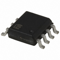
MIC5021YM Micrel Inc, MIC5021YM Datasheet - Page 5

MIC5021YM
Manufacturer Part Number
MIC5021YM
Description
IC DRIVER MOSF HI SIDE HS 8-SOIC
Manufacturer
Micrel Inc
Datasheet
1.MIC5021YM_TR.pdf
(10 pages)
Specifications of MIC5021YM
Configuration
High-Side
Input Type
Non-Inverting
Delay Time
500ns
Number Of Configurations
1
Number Of Outputs
1
Voltage - Supply
12 V ~ 36 V
Operating Temperature
-40°C ~ 85°C
Mounting Type
Surface Mount
Package / Case
8-SOIC (3.9mm Width)
Device Type
High Side
Module Configuration
High Side
Input Delay
500ns
Output Delay
800ns
Supply Voltage Range
12V To 36V
Driver Case Style
SOIC
No. Of Pins
8
Number Of Drivers
1
Driver Configuration
Non-Inverting
Driver Type
High Side
Input Logic Level
TTL
Rise Time
500ns
Fall Time
500ns
Frequency (max)
150MHz
Operating Supply Voltage (max)
36V
Operating Supply Voltage (min)
12V
Turn Off Delay Time
1.5ps
Turn On Delay Time (max)
1ns
Operating Temp Range
-40C to 85C
Operating Temperature Classification
Industrial
Mounting
Surface Mount
Pin Count
8
Lead Free Status / RoHS Status
Lead free / RoHS Compliant
Current - Peak
-
High Side Voltage - Max (bootstrap)
-
Lead Free Status / RoHS Status
Compliant, Lead free / RoHS Compliant
Other names
576-2354
MIC5021YM
MIC5021YM
Available stocks
Company
Part Number
Manufacturer
Quantity
Price
Company:
Part Number:
MIC5021YM
Manufacturer:
ROHM
Quantity:
7 167
Part Number:
MIC5021YM
Manufacturer:
MICREL/麦瑞
Quantity:
20 000
Functional Description
Refer to the MIC5021 block diagram.
Input
A signal greater than 1.4V (nominal) applied to the MIC5021
INPUT
turning the MOSFET on.
An internal pull-down resistor insures that an open
remains low, keeping the external MOSFET turned off.
Gate Output
Rapid rise and fall times on the
because each input state change triggers a one-shot which
activates a high-value current sink (10I
This draws a high current though a current mirror circuit
causing the output transistors to quickly charge or discharge
the external MOSFET’s gate.
A second current sink continuously draws the lower value
of current used to maintain the gate voltage for the selected
state.
An internal charge pump utilizes an external “boost” capacitor
connected between V
MOSFET. (Refer to typical application.) The boost capacitor
stores charge when the MOSFET is off. As the MOSFET
turns on, its source to ground voltage increases and is added
to the voltage across the capacitor, raising the V
voltage. The boost capacitor charge is directed through
the
maximum above V
the gate voltage.
Applications Information
The MIC5021 MOSFET driver is intended for high-side
switching applications where overcurrent limiting and high
speed are required. The MIC5021 can control MOSFETs
that switch voltages up to 36V.
High-Side Switch Circuit Advantages
High-side switching allows more of the load related com-
ponents and wiring to remain near ground potential when
compared to low-side switching. This reduces the chances
of short-to-ground accidents or failures.
Speed Advantage
The MIC5021 is about two orders of magnitude faster than
the low cost MIC5014 making it suitable for high-frequency
high-efficiency circuit operation in PWM (pulse width modu-
lation) designs used for motor control, SMPS (switch mode
power supply) and heating element control.
Switched loads (on/off) benefit from the MIC5021’s fast
switching times by allowing use of MOSFETs with smaller
safe operating areas. (Larger MOSFETs are often required
when using slower drivers.)
July 2005
MIC5021
GATE
causes gate enhancement on an external MOSFET
pin to quickly charge the MOSFET’s gate to 16V
DD
. The internal charge pump maintains
BOOST
and the source of the external
GATE
output are possible
2
) for a short time.
BOOST
INPUT
pin
5
An internal zener diode protects the external MOSFET by
limiting the gate to source voltage.
Sense Inputs
The MIC5021’s 50mV (nominal) trip voltage is created by
internal current sources that force approximately 5µA out of
SENSE
When
steals base current from an internal drive transistor shutting
off the external MOSFET.
Overcurrent Limiting
Current source I
external capacitor connected to C
a MOSFET Q1.
A fault condition (> 50mV from
the overcurrent comparator to enable current sink 2I
overcomes current source I
time. When C
turns off the gate output, and C
charged.
When the gate output turns the MOSFET off, the overcurrent
signal is removed from the sense inputs which deactivates
current sink 2I
connected to C
retry while the capacitor(s) recharge. Retry delay is increased
by connecting a capacitor to C
The retry cycle will continue until the fault is removed or the
input is changed to TTL low.
If C
Supply Voltage
The MIC5021’s supply input (V
supply voltage must be equal to or greater than the voltage
applied to the drain of the external N-channel MOSFET.
A 16V minimum supply is recommended to produce continu-
ous on-state, gate drive voltage for standard MOSFETs (10V
nominal gate enhancement).
When the driver is powered from a 12V to 16V supply, a
logic-level MOSFET is recommended (5V nominal gate
enhancement).
PWM operation may produce satisfactory gate enhancement
at lower supply voltages. This occurs when fast switching
repetition makes the boost capacitor a more significant volt-
age supply than the internal charge pump.
T
is connected to ground, the circuit will not retry upon a
SENSE
+ and approximately 15µA (at trip) out of
INT
– is 50mV or more below
1
. This allows C
T
1
is discharged, the
to recharge. A Schmitt trigger delays the
charges C
INT
1
to discharge C
INT
SENSE
T
DD
upon power up. An optional
INT
(optional).
T
and the optional capacitor
is kept discharged through
) is rated up to 36V. The
INPUT
and C
+ to
SENSE
is disabled, which
T
SENSE
are ready to be
INT
+,
Micrel, Inc.
in a short
–) causes
SENSE
MIC5021
SENSE
1
which
–.
–


