ADP3419JRM-REEL ON Semiconductor, ADP3419JRM-REEL Datasheet
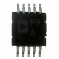
IC MOSFET DVR DUAL BOOTST 10MSOP

ADP3419JRM-REEL

Manufacturer Part Number
ADP3419JRM-REEL
Description
IC MOSFET DVR DUAL BOOTST 10MSOP
Manufacturer
ON Semiconductor
Datasheet

Specifications of ADP3419JRM-REEL

Configuration
High and Low Side, Synchronous
Input Type
PWM
Delay Time
32ns
Current - Peak
1A
Number Of Configurations
1
Number Of Outputs
2
High Side Voltage - Max (bootstrap)
30V
Voltage - Supply
4.6 V ~ 6 V
Operating Temperature
0°C ~ 100°C
Mounting Type
Surface Mount
Package / Case
10-MSOP, Micro10™, 10-uMAX, 10-uSOP
Lead Free Status / RoHS Status
Contains lead / RoHS non-compliant
Other names
ADP3419JRM-REELCT
ADP3419
Dual Bootstrapped, High
Voltage MOSFET Driver
with Output Disable
N-channel switching MOSFETs in nonisolated synchronous buck
power converters used to power CPUs in portable computers. The
driver impedances have been chosen to provide optimum performance
in multiphase regulators at up to 25 A per phase. The high-side driver
can be bootstrapped relative to the switch node of the buck converter
and is designed to accommodate the high voltage slew rate associated
with floating high-side gate drivers.
undervoltage lockout to hold the switches off until the driver has
sufficient voltage for proper operation, a crowbar input that turns on
the low-side MOSFET independently of the input signal state, and a
low-side MOSFET disable pin to provide higher efficiency at light
loads. The SD pin shuts off both the high-side and the low-side
MOSFETs to prevent rapid output capacitor discharge during system
shutdown.
temperature range of 0°C to 100°C and is available in a 10-lead MSOP
package.
FEATURES
APPLICATIONS
© Semiconductor Components Industries, LLC, 2010
April, 2010 − Rev. 3
The ADP3419 is a dual MOSFET driver optimized for driving two
The ADP3419 includes an anticross-conduction protection circuit,
The ADP3419 is specified over the extended commercial
All-In-One Synchronous Buck Driver
One PWM Signal Generates Both Drives
Anticross-Conduction Protection Circuitry
Output Disable Function
Crowbar Control
Synchronous Override Control
Undervoltage Lockout
Pb−Free Package is Available
Mobile Computing CPU Core Power Converters
Multiphase Desk-Note CPU Supplies
Single-Supply Synchronous Buck Converters
Non-Synchronous-to-Synchronous Drive Conversion
1
See detailed ordering and shipping information in the package
dimensions section on page 9 of this data sheet.
(Note: Microdot may be in either location)
CROWBAR
DRVLSD
ORDERING INFORMATION
VCC
SD
P9x = Device Code
R
Y
W
G
IN
MARKING DIAGRAM
http://onsemi.com
1
PIN ASSIGNMENT
1
2
3
4
5
= Assembly Location
= Year
= Work Week
= Pb−Free Package
10
x = A or B
(Top View)
ADP3419
1
RYWG
P9x
Publication Order Number:
G
CASE 846AC
MSOP−10
10
9
8
7
6
BST
DRVH
SW
GND
DRVL
ADP3419/D

Related parts for ADP3419JRM-REEL

ADP3419JRM-REEL Summary of contents

Page 1

ADP3419 Dual Bootstrapped, High Voltage MOSFET Driver with Output Disable The ADP3419 is a dual MOSFET driver optimized for driving two N-channel switching MOSFETs in nonisolated synchronous buck power converters used to power CPUs in portable computers. The driver impedances ...

Page 2

VCC BST UVLO, OVERLAP SD 2 PROTECTION, SHUTDOWN AND DRVLSD 3 CROWBAR CIRCUITS CROWBAR 4 ADP3419 7 GND Figure 1. Simplified Block Diagram ABSOLUTE MAXIMUM RATINGS Parameter VCC BST BST DRVH DRVL All ...

Page 3

PIN ASSIGNMENT Pin No. Mnemonic 1 IN Logic Level PWM Input. This pin has primary control of the drive outputs. In normal operation, pulling this pin low turns on the low-side driver; pulling it high turns on the high-side driver. ...

Page 4

IN DRVLSD DRVL Figure 3. Output Disable Timing Diagram (Timing is Referenced to the 90% and 10% Points Unless Otherwise Noted pdl f DRVL DRVL DRVL t pdh DRVH−SW SW Figure 4. Non−Overlap Timing Diagram (Timing is ...

Page 5

Figure 5. DRVH Rise and DRVL Fall Times CH1 = IN, CH2 = DRVH, CH3 = DRVL 25 VCC = 3nF LOAD 20 RISE TIME 15 FALLTIME JUNCTION TEMPERATURE (°C) ...

Page 6

VCC = 5V t DRVH pdh C = 3nF LOAD JUNCTION TEMPERATURE (°C) Figure 11. DRVH and DRVL t vs. Temperature pdh 100 ...

Page 7

Theory of Operation The ADP3419 is a dual MOSFET driver optimized for driving two N-channel MOSFETs in a synchronous buck converter topology. A single PWM input signal is all that is required to properly drive the high-side and the low-side ...

Page 8

When DRVLSD is low, the low-side driver stays low. When DRVLSD is high, the low-side driver is enabled and controlled by the driver signals, as previously described. Low-Side Driver Timeout In normal operation, the DRVH signal tracks the IN signal ...

Page 9

... VCC 5.0 V power rail. ORDERING INFORMATION Device Number ADP3419JRM−REEL ADP3419JRMZ−REEL ADP34190091RMZR †For information on tape and reel specifications, including part orientation and tape sizes, please refer to our Tape and Reel Packaging Specifications Brochure, BRD8011/D. *The “Z’’ suffix indicates Pb−Free part. ...

Page 10

... SEATING H PLANE *For additional information on our Pb−Free strategy and soldering details, please download the ON Semiconductor Soldering and Mounting Techniques Reference Manual, SOLDERRM/D. ON Semiconductor and are registered trademarks of Semiconductor Components Industries, LLC (SCILLC). SCILLC reserves the right to make changes without further notice to any products herein ...

Related keywords