ADP3419JRM-REEL ON Semiconductor, ADP3419JRM-REEL Datasheet - Page 9
ADP3419JRM-REEL
Manufacturer Part Number
ADP3419JRM-REEL
Description
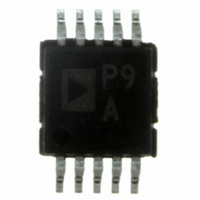
IC MOSFET DVR DUAL BOOTST 10MSOP
Manufacturer
ON Semiconductor
Datasheet
1.ADP3419JRMZ-REEL.pdf
(10 pages)
Specifications of ADP3419JRM-REEL
Configuration
High and Low Side, Synchronous
Input Type
PWM
Delay Time
32ns
Current - Peak
1A
Number Of Configurations
1
Number Of Outputs
2
High Side Voltage - Max (bootstrap)
30V
Voltage - Supply
4.6 V ~ 6 V
Operating Temperature
0°C ~ 100°C
Mounting Type
Surface Mount
Package / Case
10-MSOP, Micro10™, 10-uMAX, 10-uSOP
Lead Free Status / RoHS Status
Contains lead / RoHS non-compliant
Other names
ADP3419JRM-REELCT


to the MOSFET data sheets, Q
Q
be about 130 mW.
ADP3419. The temperature rise of the ADP3419 against its
environment is estimated as:
to air, given in the absolute maximum ratings as 220°C/W
for a 4−layer board.
R1 and R2 are the output resistances of the high-side driver:
R3 and R4 are the output resistances of the low-side driver:
R is the external resistor between the BST pin and the BST
capacitor.
R
low-side MOSFETs, respectively.
Equation 5 gives a value of η = 0.71. Based on Equation 4,
the estimated temperature rise in this example is about 22°C.
PC Board Layout Considerations
printed circuit boards. Figure 17 gives an example of the
typical land patterns based on the guidelines given here.
•
•
†For information on tape and reel specifications, including part orientation and tape sizes, please refer to our Tape and Reel Packaging
*The “Z’’ suffix indicates Pb−Free part.
ORDERING INFORMATION
Specifications Brochure, BRD8011/D.
LSGATE
HSGATE
ADP3419JRM−REEL
ADP3419JRMZ−REEL
ADP34190091RMZR
Part of this power consumption generates heat inside the
where θ
where:
Assuming that R = 0 and that R
Use the following general guidelines when designing
The VCC bypass capacitor should be located as close as
possible to the VCC and GND pins. Place the
ADP3419 and bypass capacitor on the same layer of the
board, so that the PCB trace between the ADP3419
VCC pin and the MLC capacitor does not contain any
via. An ideal location for the bypass MLC capacitor is
near Pin 5 and Pin 6 of the ADP3419.
High frequency switching noise can be coupled into the
VCC pin of the ADP3419 via the BST diode.
Therefore, do not connect the anode of the BST diode
to the VCC pin with a short trace. Use a separate via or
trace to connect the anode of the BST diode directly to
the VCC 5.0 V power rail.
R1 = 1.7 (DRVH − BST), R2 = 0.8 (DRVH − SW).
R3 = 1.7 (DRVL − VCC), R4 = 0.8 (DRVL − GND).
= 68 nC. Given that f
and R
JA
Device Number
is ADP3419’s thermal resistance from junction
LSGATE
DT [ q
are gate resistances of high-side and
JA
h [
MAX
P
Q
)
MAX
HSGATE
HSGATE
HSGATE
Q
is 300 kHz, P
HSGATE
Q
HSGATE
h
Q
) Q
= R
LSGATE
= 18.6 nC and
Branding
) Q
LSGATE
P9A
P9B
P9B
LSGATE
MAX
LSGATE
(eq. 4)
http://onsemi.com
would
= 0.5,
R1 ) R
R3 ) R
9
0.5
0.5
resistance of ADP3419 and in the MOSFET gate resistance
as well. η represents the ratio of power dissipation inside the
ADP3419 over the total MOSFET gate driving power. For
normal applications, a rough estimation for η is 0.7. A more
accurate estimation can be calculated using:
•
•
HSGATE
10−Lead MSOP
10−Lead MSOP
10−Lead MSOP
Package Type
Figure 17. External Component Placement Example
The total MOSFET drive power dissipates in the output
It is best to have the low-side MOSFET gate close to
the DRVL pin; otherwise, use a short and very thick
PCB trace between the DRVL pin and the low-side
MOSFET gate.
Fast switching of the high-side MOSFET can reduce
switching loss. However, EMI problems can arise due
to the severe ringing of the switch node voltage.
Depending on the character of the low-side MOSFET, a
very fast turn-on of the high-side MOSFET may falsely
turn on the low-side MOSFET through the dv/dt
coupling of its Miller capacitance. Therefore, when fast
turn-on of the high-side MOSFET is not required by the
application, a resistor of about 1 W to 2 W can be placed
between the BST pin and the BST capacitor to limit the
turn-on speed of the high-side MOSFET.
LSGATE
R1
R3
) R
)
)
R4 ) R
C
VCC
R2 ) R
0.5
D1
0.5
LSGATE
R4
HSGATE
R2
R
BST
3000 Tape & Reel
3000 Tape & Reel
3000 Tape & Reel
SHORT, THICK TRACE
TO THE GATES OF
LOW-SIDE MOSFETS
Shipping
C
BST
†
TO SWITCH
NODE
(eq. 5)
Related parts for ADP3419JRM-REEL
Image
Part Number
Description
Manufacturer
Datasheet
Request
R

Part Number:
Description:
ON Semiconductor [VOLTAGE REGULATOR]
Manufacturer:
ON Semiconductor
Datasheet:
Part Number:
Description:
357-036-542-201 CARDEDGE 36POS DL .156 BLK LOPRO
Manufacturer:
ON Semiconductor
Datasheet:
Part Number:
Description:
357-036-542-201 CARDEDGE 36POS DL .156 BLK LOPRO
Manufacturer:
ON Semiconductor
Datasheet:
Part Number:
Description:
357-036-542-201 CARDEDGE 36POS DL .156 BLK LOPRO
Manufacturer:
ON Semiconductor
Datasheet:
Part Number:
Description:
357-036-542-201 CARDEDGE 36POS DL .156 BLK LOPRO
Manufacturer:
ON Semiconductor
Datasheet:
Part Number:
Description:
357-036-542-201 CARDEDGE 36POS DL .156 BLK LOPRO
Manufacturer:
ON Semiconductor
Datasheet:
Part Number:
Description:
357-036-542-201 CARDEDGE 36POS DL .156 BLK LOPRO
Manufacturer:
ON Semiconductor
Datasheet:
Part Number:
Description:
357-036-542-201 CARDEDGE 36POS DL .156 BLK LOPRO
Manufacturer:
ON Semiconductor
Datasheet:
Part Number:
Description:
357-036-542-201 CARDEDGE 36POS DL .156 BLK LOPRO
Manufacturer:
ON Semiconductor
Datasheet:
Part Number:
Description:
357-036-542-201 CARDEDGE 36POS DL .156 BLK LOPRO
Manufacturer:
ON Semiconductor
Datasheet:
Part Number:
Description:
357-036-542-201 CARDEDGE 36POS DL .156 BLK LOPRO
Manufacturer:
ON Semiconductor
Datasheet:
Part Number:
Description:
Manufacturer:
ON Semiconductor
Datasheet:
Part Number:
Description:
Manufacturer:
ON Semiconductor
Datasheet:
Part Number:
Description:
Manufacturer:
ON Semiconductor
Datasheet: