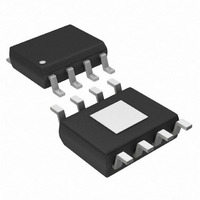
MAX5056AASA+ Maxim Integrated Products, MAX5056AASA+ Datasheet - Page 2

MAX5056AASA+
Manufacturer Part Number
MAX5056AASA+
Description
IC MOSFET DRVR DUAL 8-SOIC
Manufacturer
Maxim Integrated Products
Type
Low Sider
Datasheet
1.MAX5054AATAT.pdf
(15 pages)
Specifications of MAX5056AASA+
Configuration
Low-Side
Input Type
Non-Inverting
Delay Time
20ns
Current - Peak
4A
Number Of Configurations
2
Number Of Outputs
2
Voltage - Supply
4 V ~ 15 V
Operating Temperature
-40°C ~ 125°C
Mounting Type
Surface Mount
Package / Case
8-SOIC (3.9mm Width) Exposed Pad, 8-eSOIC. 8-HSOIC
Rise Time
85 ns
Fall Time
75 ns
Supply Voltage (min)
4 V
Supply Current
2.4 mA
Maximum Power Dissipation
1538 mW
Maximum Operating Temperature
+ 125 C
Mounting Style
SMD/SMT
Maximum Turn-off Delay Time
35 ns
Maximum Turn-on Delay Time
35 ns
Minimum Operating Temperature
- 40 C
Number Of Drivers
2
Lead Free Status / RoHS Status
Lead free / RoHS Compliant
High Side Voltage - Max (bootstrap)
-
Lead Free Status / Rohs Status
Lead free / RoHS Compliant
ABSOLUTE MAXIMUM RATINGS
(Voltages referenced to GND.)
V
INA+, INA-, INB+, INB- ...............................................-0.3V to +18V
OUTA, OUTB...................................................-0.3V to (V
OUTA, OUTB Short-Circuit Duration ........................................10ms
Continuous Source/Sink Current at OUT_ (P
Continuous Power Dissipation (T
PACKAGE THERMAL CHARACTERISTICS (Note 1)
8 TDFN-EP
8 SO
4A, 20ns, Dual MOSFET Drivers
Stresses beyond those listed under “Absolute Maximum Ratings” may cause permanent damage to the device. These are stress ratings only, and functional
operation of the device at these or any other conditions beyond those indicated in the operational sections of the specifications is not implied. Exposure to
absolute maximum rating conditions for extended periods may affect device reliability.
Note 1: Package thermal resistances were obtained using the method described in JEDEC specification JESD51-7, using a four-
ELECTRICAL CHARACTERISTICS
(V
2
POWER SUPPLY
V
V
V
Hysteresis
V
Output Delay
V
DRIVER OUTPUT (SINK)
Driver Output Resistance Pulling
Down
Peak Output Current (Sinking)
Output-Voltage Low
Latchup Protection
DD
Junction-to-Ambient Thermal Resistance (
Junction-to-Case Thermal Resistance (
Junction-to-Ambient Thermal Resistance (
Junction-to-Case Thermal Resistance (
8-Pin TDFN-EP (derate 18.2mW/°C above +70°C)........1454mW
DD
DD
DD
DD
DD
DD
...............................................................................-0.3V to +18V
_______________________________________________________________________________________
= 4V to 15V, T
Operating Range
Undervoltage Lockout
Undervoltage Lockout
Undervoltage Lockout to
Supply Current
layer board. For detailed information on package thermal considerations, refer to www.maxim-ic.com/thermal-tutorial.
PARAMETER
A
= -40°C to +125°C, unless otherwise noted. Typical values are at V
A
= +70°C)
SYMBOL
JC
JC
I
R
UVLO
DD-SW
I
).......................+40°C/W
V
I
D
PK-N
ON-N
JA
I
LUP
)......................+8°C/W
DD
JA
DD
< P
)................+132°C/W
)...............+41°C/W
DMAX
V
V
INA- = INB- = V
INA+ = INB+ = 0V
(not switching)
INA- = 0V, INB+ = V
INA+ = INB- both channels switching at
250kHz, C
V
I
V
I
V
I
Reverse current I
OUT_
OUT_
OUT_
DD
DD
DD
DD
DD
) .....200mA
DD
rising
rising
= 15V,
= 4.5V,
= 15V, C
+ 0.3V)
= -100mA
= -100mA
= -100mA
L
= 0F
L
CONDITIONS
= 10,000pF
DD
OUT_
,
Operating Temperature Range..............................-40°C to +125°C
Storage Temperature Range .................................-65°C to +150°C
Junction Temperature ...........................................................+150°C
Lead Temperature (soldering, 10s)......................................+300°C
Soldering Temperature (reflow)............................................+260°C
8 SO-EP
DD
Junction-to-Ambient Thermal Resistance (
Junction-to-Case Thermal Resistance (
8-Pin SO-EP (derate 19.2mW/°C above +70°C)… ........1538mW
8-Pin SO (derate 5.9mW/°C above +70°C)… ..................471mW
(Note 2)
= 15V,
V
V
T
T
T
T
V
V
A
A
A
A
DD
DD
DD
DD
= +25°C
= +125°C
= +25°C
= +125°C
= 4V
= 15V
= 4.5V
= 15V
DD
= 15V and T
MIN
3.00
400
4
1
A
= +25 C.) (Note 2)
TYP
3.50
200
2.4
1.1
1.5
2.2
3.0
12
28
40
4
JC
JA
)......................+7°C/W
)..................+41°C/W
MAX
3.85
0.45
0.24
1.8
2.4
3.3
4.5
15
55
75
4
UNITS
mV
mA
mA
µA
µs
V
V
A
V


