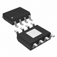
MAX5056AASA+ Maxim Integrated Products, MAX5056AASA+ Datasheet - Page 8

MAX5056AASA+
Manufacturer Part Number
MAX5056AASA+
Description
IC MOSFET DRVR DUAL 8-SOIC
Manufacturer
Maxim Integrated Products
Type
Low Sider
Datasheet
1.MAX5054AATAT.pdf
(15 pages)
Specifications of MAX5056AASA+
Configuration
Low-Side
Input Type
Non-Inverting
Delay Time
20ns
Current - Peak
4A
Number Of Configurations
2
Number Of Outputs
2
Voltage - Supply
4 V ~ 15 V
Operating Temperature
-40°C ~ 125°C
Mounting Type
Surface Mount
Package / Case
8-SOIC (3.9mm Width) Exposed Pad, 8-eSOIC. 8-HSOIC
Rise Time
85 ns
Fall Time
75 ns
Supply Voltage (min)
4 V
Supply Current
2.4 mA
Maximum Power Dissipation
1538 mW
Maximum Operating Temperature
+ 125 C
Mounting Style
SMD/SMT
Maximum Turn-off Delay Time
35 ns
Maximum Turn-on Delay Time
35 ns
Minimum Operating Temperature
- 40 C
Number Of Drivers
2
Lead Free Status / RoHS Status
Lead free / RoHS Compliant
High Side Voltage - Max (bootstrap)
-
Lead Free Status / Rohs Status
Lead free / RoHS Compliant
4A, 20ns, Dual MOSFET Drivers
MAX5054
MAX5055/MAX5056/MAX5057
8
MAX5055
_______________________________________________________________________________________
1, 8
—
—
—
2
3
4
5
6
7
PIN
—
1
2
3
4
5
6
7
8
MAX5056 MAX5057
PIN
1, 8
—
—
—
3
5
6
7
4
2
NAME
OUTB
OUTA
GND
INB+
INA+
INA-
INB-
V
EP
DD
1, 8
—
—
—
2
3
5
6
7
4
Inverting Logic-Input Terminal for Driver A. Connect to GND when not used.
Inverting Logic-Input Terminal for Driver B. Connect to GND when not used.
Ground
Driver B Output. Sources or sinks current for channel B to turn the external MOSFET on or off.
Power Supply. Bypass to GND with one or more 0.1µF ceramic capacitors.
Driver A Output. Sources or sinks current for channel A to turn the external MOSFET on or off.
Noninverting Logic-Input Terminal for Driver B. Connect to V
Noninverting Logic-Input Terminal for Driver A. Connect to V
Exposed Pad. Internally connected to GND. Do not use the exposed pad as the only electrical
ground connection.
NAME
OUTB
OUTA
INB+
INA+
GND
N.C.
INA-
INB-
V
EP
DD
No Connection. Not internally connected.
Inverting Logic-Input Terminal for Driver A. Connect to GND if not used.
Ground
Inverting Logic-Input Terminal for Driver B. Connect to GND if not used.
Driver B Output. Sources or sinks current for channel B to turn the external
MOSFET on or off.
Power Supply. Bypass to GND with one or more 0.1µF ceramic capacitors.
Driver A Output. Sources or sinks current for channel A to turn the external
MOSFET on or off.
Noninverting Logic-Input Terminal for Driver B. Connect to V
Noninverting Logic-Input Terminal for Driver A. Connect to V
Exposed Pad. Internally connected to GND. Do not use the exposed pad as
the only electrical ground connection.
FUNCTION
FUNCTION
DD
DD
when not used.
when not used.
Pin Descriptions
DD
DD
if not used.
if not used.


