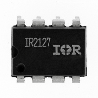
IR2127 International Rectifier, IR2127 Datasheet

IR2127
Specifications of IR2127
Available stocks
Related parts for IR2127
IR2127 Summary of contents
Page 1
... FAULT CS FAULT COM V S IR2127/IR21271 (Refer to Lead Assignments for correct pin configuration). This/These diagram(s) show electrical connections only. Please refer to our Application Notes and DesignTips for proper circuit board layout. www.irf.com IR2127 ( IR2128 ( S ) IR21271 ( S ) & (PbF) signal is pro- 8-Lead PDIP FAULT ...
Page 2
... Current Sense Signal Voltage CS T Ambient Temperature A Note 1: Logic operational for +600V. Logic state held for V S DT97-3 for more details). 2 Definition ≤ +25°C (8 Lead DIP Lead SOIC) (8 Lead DIP) (8 Lead SOIC) Definition (IR2127/IR2128) (IR21271 Min. Max. Units -0.3 625 ...
Page 3
... V — — O BIAS — — O — — — 200 — 60 — 7.0 — — — — — — (IR2127/IR2128) 8.8 10.3 (IR21271) 6.3 7.2 (IR2127/IR2128) 7.5 9.0 (IR21271) 6.0 6.8 200 250 420 500 — 125 250 200 V = 600V S 130 65 ...
Page 4
... Functional Block Diagram IR2127/IR21271 FAULT COM Functional Block Diagram IR2128 FAULT COM 4 UV DETECT R HV LEVEL R PULSE UP SHIFT FILTER SHIFTERS S PULSE V B GEN PULSE GEN DOWN SHIFTER PULSE FILTER UV DETECT R HV LEVEL R PULSE UP SHIFT FILTER SHIFTERS S PULSE V B GEN PULSE GEN ...
Page 5
... Lead Definitions Symbol Description V Logic and gate drive supply CC IN Logic input for gate driver output (HO), in phase with HO (IR2127/IR21271) Indicates over-current shutdown has occurred, negative logic FAULT COM Logic ground V High side floating supply B High side gate drive output HO V High side floating supply return ...
Page 6
... Figure 4. CS Shutdown Waveform Definitions 6 IN 50% 50% (IR2128) 50% 50% IN (IR2127 off IR21271) 90% HO 10% Figure 2. Switching Time Waveform Definition IN 50% (IR2128) 50 (IR2127/ bl IR21271) CS 90% HO FAULT Figure 3. Start-up Blanking Time Waveform Definitions V CSTH CS t flt FAULT 90% Figure FAULT Waveform Definitions t f 90% 10% www.irf.com ...
Page 7
Max. 200 100 Typ 0 -50 - Tem pe rature (°C) o Temperature ( C) Figure 10A Turn-On Time vs. Temperature 350 300 250 200 150 100 ...
Page 8
Max 100 . Typ 0 -50 - Temperature ( Tem perature (°C) C) Figure 12A Turn-On Rise Time vs. Temperature 200 150 100 Max. 50 Typ 0 . -50 -25 0 ...
Page 9
... Figure 16B CS to FAULT Pull-Up Propagation Delay Min 100 125 10 Figure 17B Logic “1” Input Voltage (IR2127) M AX. Typ Vcc Supply Voltage(V) Vcc Supply Voltage (V) vs. Voltage VCC Supply Voltage (V) vs. Voltage VCC Supply Voltage (V) VCC Supply Voltage (V) Logic “ ...
Page 10
... Temperature ( C) Figure 20A High Level Output vs Temperature 10 4 3.2 2 100 125 Figure 18B Logic “0” Input Voltage (IR2127) 500 400 Max. 300 200 Typ. 100 Min 100 125 10 Figure 19B CS Input Positive Going Voltage 1 0.8 0.6 0.4 Max. ...
Page 11
Max. 0.2 0 -50 - Temperature ( C) Figure 21A Low Level Output vs Temperature 500 400 300 200 100 Max. 0 -50 - Temperature ( C) Figure ...
Page 12
Max . 150 Typ 100 . 50 0 -50 - Temperature ( C) Figure 24A Vcc Supply Current vs Temperature Max Typ 0 -50 -25 ...
Page 13
... Figure 27B “High” CS Bias Current Max 100 125 10 Figure 28B “Low” CS Bias Current vs Voltage Max Typ 100 125 10 Figure 29B VBS Undervoltage Threshold (+) Vcc Supply Voltage (V) vs Voltage VCC Supply Voltage ( VCC Supply Voltage (V) Vcc Supply Voltage (V) vs Voltage (IR2127/IR2128 ...
Page 14
... Figure 31B Output Source Current vs Voltage 800 700 600 500 400 300 200 100 0 75 100 125 Figure 32B Output Sink Current vs Voltage Max. Typ. Min Vcc Supply Voltage (V) vs Voltage (IR2127/IR2128 VBIAS Supply Voltage (V) Typ. Min VBIAS Supply Voltage (V) www.irf.com ...
Page 15
Case outlines 0.25 [.010 0.25 [.010 NOT DIMENSIONING & TOLE RANCING PER AS ...
Page 16
... Lead-Free Part 8-Lead PDIP IR2127 8-Lead SOIC IR2127S 8-Lead PDIP IR21271 8-Lead SOIC IR21271S order IR21271SPbF 8-Lead PDIP IR2128 8-Lead SOIC IR2128S This product has been designed and qualified for the Industrial market. Qualification Standards can be found on IR’s Web site. ...


