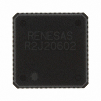
R2J20602NP#G3 Renesas Electronics America, R2J20602NP#G3 Datasheet

R2J20602NP#G3
Specifications of R2J20602NP#G3
Available stocks
Related parts for R2J20602NP#G3
R2J20602NP#G3 Summary of contents
Page 1
To our customers, Old Company Name in Catalogs and Other Documents st On April 1 , 2010, NEC Electronics Corporation merged with Renesas Technology Corporation, and Renesas Electronics Corporation took over all the business of both companies. Therefore, although the ...
Page 2
All information included in this document is current as of the date this document is issued. Such information, however, is subject to change without any prior notice. Before purchasing or using any Renesas Electronics products listed herein, please confirm ...
Page 3
R2J20602NP Integrated Driver – MOS FET (DrMOS) Description The R2J20602NP multi-chip module incorporates a high-side MOS FET, low-side MOS FET, and MOS-FET driver in a single QFN package. The on and off timing of the power MOS FET is optimized ...
Page 4
R2J20602NP Block Diagram DISBL# 2 µA CGND VCIN Input logic (TTL level) PWM (3 state in) CGND Notes: 1. Truth table for the DISBL# pin. DISBL# Input “L” Shutdown (GL “L”) “Open” Shutdown (GL “L”) “H” ...
Page 5
R2J20602NP Pin Arrangement VIN 15 VIN 16 VIN 17 VIN 18 VIN 19 VIN 20 VSWH 21 PGND 22 PGND 23 PGND 24 PGND 25 PGND 26 PGND 27 PGND 28 Note: All die-pads (three pads in total) should be ...
Page 6
R2J20602NP Absolute Maximum Ratings Item Power dissipation Average output current Input voltage Supply voltage Low side driver voltage Switch node voltage BOOT voltage DISBL# voltage PWM voltage Reg5V current Operating junction temperature Storage temperature Notes: 1. Pt(25) represents a PCB ...
Page 7
R2J20602NP Electrical Characteristics (Ta = 25C, VCIN = 12 V, VLDRV = 5 V, VSWH = 0 V, unless otherwise specified) Item Supply VCIN start threshold VCIN shutdown threshold UVLO hysteresis VCIN bias current VLDRV bias current PWM PWM rising ...
Page 8
R2J20602NP Typical Application + +12 V PWM1 PWM PWM2 control circuit PWM3 PWM4 REJ03G1480-0500 Rev.5.00 Mar 12, 2010 Page VCIN VLDRV BOOT DISBL# VIN Reg5V VSWH R2J20602NP PWM PGND CGND GH ...
Page 9
R2J20602NP Test Circuit LDRV VLDRV A I CIN VCIN pulse × V Note LDRV × OUT O O Efficiency = ...
Page 10
R2J20602NP Typical Data Power Loss vs. Output Current 12 VIN = VCIN = 12 V VLDRV = VOUT = 1 MHz PWM L = 0.45 µ ...
Page 11
R2J20602NP Typical Data (cont.) Power Loss vs. Output Inductance 1.20 1.15 1.10 1.05 1.00 0.95 VIN = 12 V VCIN = 12 V 0.90 VLDRV = 5 V VOUT = 1 MHz 0.85 PWM Iout = ...
Page 12
R2J20602NP Description of Operation The DrMOS multi-chip module incorporates a high-side MOS FET, low-side MOS FET, and MOS-FET driver in a single QFN package. Since the parasitic inductance between each chip is extremely small, the module is highly suitable for ...
Page 13
R2J20602NP The PWM input is TTL level and has hysteresis. When the PWM input signal is abnormal, e.g., when the signal route from the control IC is abnormal, the tri-state function turns off the high- and low-side MOS FETs. This ...
Page 14
R2J20602NP PCB Layout Example Figure 2 shows an example of a PCB layout for the R2J20602NP in application. The several ceramic capacitors (e.g. 10 F) close to VIN and PGND can be expected to decrease switching noise and improve efficiency. ...
Page 15
R2J20602NP Footprint Example 4.30 3.60 3.10 0.45 0.90 3. REJ03G1480-0500 Rev.5.00 Mar 12, 2010 Page 0.5 Figure 3 Footprint Example (Unit: mm) ...
Page 16
... R2J20602NP Package Dimensions JEITA Package Code RENESAS Code P-HVQFN56-8x8-0.50 PVQN0056KA Index mark y Ordering Information Part Name R2J20602NP#G3 REJ03G1480-0500 Rev.5.00 Mar 12, 2010 Page Previous Code MASS[Typ.] — 0. Quantity 2500 pcs 42 43 3.0 0.0 0.3 1.0 Dimension in Millimeters Reference Symbol Min Nom Max 3 ...
Page 17
Notes: 1. This document is provided for reference purposes only so that Renesas customers may select the appropriate Renesas products for their use. Renesas neither makes warranties or representations with respect to the accuracy or completeness of the information contained ...


