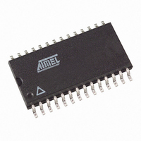
T6816-TIQY Atmel, T6816-TIQY Datasheet

T6816-TIQY
Specifications of T6816-TIQY
T6816-TIQYTR
Available stocks
Related parts for T6816-TIQY
T6816-TIQY Summary of contents
Page 1
... SO28 Power Package 1. Description The T6816 is a fully protected driver interface designed in 0.8 µm BCDMOS technol- ogy especially suitable for truck or bus applications and the industrial 24-V supply. It controls different loads via a 16-bit dataword. Each of the six high-side and six low-side drivers is capable to drive currents up to 600 mA ...
Page 2
... Figure 1-1. Block Diagram HS1 15 15 Fault Detect CLK Input Register 24 CS Output Register INH Fault Detect 16 LS1 T6816 2 HS3 HS2 HS4 Fault Fault Fault Detect Detect Detect Fault Fault Fault Detect Detect Detect 14 11 LS2 LS3 LS4 HS5 HS6 2 28 ...
Page 3
... LS6 Low-side driver output 6; see pin 1 28 HS6 High-side driver output 6; see pin 2 4595G–BCD–04/09 DI CLK CS GND GND GND T6816 Lead frame GND GND GND HS4 LS4 VS GND VCC DO INH LS1 HS1 GND VS LS3 HS3 HS2 LS2 = 2 MHz) max T6816 3 ...
Page 4
... SLS1 SHS1 SLS2 SHS2 SLS3 SHS3 SLS4 SHS4 SLS5 SHS5 SLS6 SHS6 SCD Table 3-1. Bit T6816 4 LS2 HS2 LS3 HS3 LS4 HS4 Input Data Protocol Input Register Function Status register reset (high = reset; the bits PSF, SCD and SRR overtemperature shutdown in the output data register are set to low) ...
Page 5
... High = standby, low = normal operation PSF Power supply fail: undervoltage at pin VS detected Bit high: overtemperature shutdown Bit 11 Bit 10 Bit 9 Bit 8 Bit 7 (LS6) (HS5) (LS5) (HS4) (LS4 Bit 6 Bit 5 Bit 4 Bit 3 Bit 2 (HS3) (LS3) (HS2) (LS2) (HS1 T6816 Bit 1 Bit 0 (LS1) (SRR ...
Page 6
... SRR bit in the input register, the SCD bit is reset and the disabled outputs are enabled. 3.6 Inhibit There are two ways to inhibit the T6816: 1. Set bit SI in the input register to zero 2. Switch pin 17 (INH both cases, all output stages are turned off but the serial interface stays active. The output stages can be activated again by bit pin 17 (INH) switched back to 5V ...
Page 7
... CLK, CS –10 to +10 Internal limited, see LS6 output specification HS6 –0.3 to +40 17 HS6 –40 to +150 j –55 to +150 Min. Typ. Max Min. Typ. Max. ( 4.5 5 5.5 V CLK, –0.3 V VCC 2 –40 150 j T6816 Unit °C °C Unit K/W K/W Unit MHz °C 7 ...
Page 8
... Thermal shutdown *) Type means: A =100% tested 100% correlation tested Characterized on samples Design parameter Notes: 1. Delay time between rising edge of CS after data transmission and switch on output stages to 90% of final level T6816 8 Test Conditions ISO 7637-1 VDE 0879 Part 2 MIL-STD-883D Method 3015.7 EOS/ESD - S 5.2 < ...
Page 9
... I LS1-6 16 12, 13 15, I HS1-6 28 Min. Typ. Max. 130 150 170 20 1.05 1.17 1.05 1.2 1.5 2 –10 15 /dt 50 200 400 /dt 650 950 1250 –1250 –950 –650 1.0 1.5 2.0 60 200 –150 –30 T6816 Unit Type* ° µA A µ mV/µ µA A µ ...
Page 10
... V *) Type means: A =100% tested 100% correlation tested Characterized on samples Design parameter Notes: 1. Delay time between rising edge of CS after data transmission and switch on output stages to 90% of final level T6816 10 < 150°C; unless otherwise specified, all values refer to GND pins. j ...
Page 11
... DO = 100 – Symbol Min. Typ. Max. t 200 ENDO t 200 DISDO t 100 DOf t 100 DOr t 200 DOVal t 225 CSSethl t 225 CSSetlh t 16 CSh t 2 CSh t 225 CLKh t 225 CLKl t 500 CLKp t 225 CLKSethl t 225 CLKSetlh t 40 DIset t 40 DIHold T6816 Unit ...
Page 12
... Figure 9-1. Serial Interface Timing with Chart Numbers CLK 3 DI CLK DO Inputs DI, CLK, CS: High level = 0.7 Output DO: High level = 0.8 T6816 low level = 0 low level = 0 4595G–BCD–04/09 ...
Page 13
... Absolute Maximum Ratings). HSX CC HS5 HS6 Fault Fault S Detect Detect GND Osc 7 S GND GND UV - Control protection logic 9 GND Thermal protection GND Power-on 21 Reset GND GND Fault Fault 23 GND Detect Detect LS5 LS6 V S and T6816 BYT41D Batt 24V + close as possi ...
Page 14
... Ordering Information Extended Type Number T6816-TIQY 12. Package Information Package SO28 Dimensions in mm 0.4 1. T6816 14 Package SO28 18.05 17.80 0.25 0.10 16. Remarks Power package, taped and reeled, Pb-free 9.15 8.65 7.5 7.3 2.35 10.50 10.20 technical drawings according to DIN specifications 0.25 4595G–BCD–04/09 ...
Page 15
... Section 1 “Description” on page 1 changed Ordering Information on page 14 changed Put datasheet in a new template Table “Electrical Characteristics” rows 5.15 and 5.16 changed Put datasheet in a new template Table “Absolute Maximum Ratings” on page 7 changed Table “Electrical Characteristics” on page 10 changed T6816 15 ...
Page 16
... Disclaimer: The information in this document is provided in connection with Atmel products. No license, express or implied, by estoppel or otherwise, to any intellectual property right is granted by this document or in connection with the sale of Atmel products. EXCEPT AS SET FORTH IN ATMEL’S TERMS AND CONDI- TIONS OF SALE LOCATED ON ATMEL’S WEB SITE, ATMEL ASSUMES NO LIABILITY WHATSOEVER AND DISCLAIMS ANY EXPRESS, IMPLIED OR STATUTORY WARRANTY RELATING TO ITS PRODUCTS INCLUDING, BUT NOT LIMITED TO, THE IMPLIED WARRANTY OF MERCHANTABILITY, FITNESS FOR A PARTICULAR PURPOSE, OR NON-INFRINGEMENT ...


