T6816-TIQY Atmel, T6816-TIQY Datasheet - Page 4
T6816-TIQY
Manufacturer Part Number
T6816-TIQY
Description
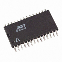
IC DRIVER HEX DUAL 24V 28-SOIC
Manufacturer
Atmel
Type
High Side/Low Side Driverr
Datasheet
1.T6816-TIQY.pdf
(16 pages)
Specifications of T6816-TIQY
Input Type
Serial
Number Of Outputs
12
On-state Resistance
2 Ohm, 1.5 Ohm
Current - Output / Channel
600mA
Current - Peak Output
950mA
Voltage - Supply
7 V ~ 40 V
Operating Temperature
-40°C ~ 150°C
Mounting Type
Surface Mount
Package / Case
28-SOIC (7.5mm Width)
Product
H-Bridge Drivers
Maximum Operating Temperature
+ 150 C
Mounting Style
SMD/SMT
Minimum Operating Temperature
- 40 C
For Use With
ATAB6816 - BOARD EVAL FOR T6816/U6815BM
Lead Free Status / RoHS Status
Lead free / RoHS Compliant
Other names
T6816-TIQY
T6816-TIQYTR
T6816-TIQYTR
Available stocks
Company
Part Number
Manufacturer
Quantity
Price
Company:

Part Number:
T6816-TIQY
Manufacturer:
SIEMENS
Quantity:
1 100
Part Number:
T6816-TIQY
Manufacturer:
TFK
Quantity:
20 000


3. Functional Description
3.1
Figure 3-1.
4
Serial Interface
CS
DI
CLK
DO
T6816
Data Transfer Input Data Protocol
TP
SRR
0
SLS1 SHS1 SLS2 SHS2 SLS3 SHS3 SLS4 SHS4 SLS5 SHS5 SLS6 SHS6 SCD
1
LS1
Data transfer starts with the falling edge of the CS signal. Data must appear at DI synchronized
to CLK and are accepted on the falling edge of the CLK signal. LSB (bit 0, SRR) has to be trans-
ferred first. Execution of new input data is enabled on the rising edge of the CS signal. When CS
is high, pin DO is in tri-state condition. This output is enabled on the falling edge of CS. Output
data will change their state with the rising edge of CLK and stay stable until the next rising edge
of CLK appears. LSB (bit 0, TP) is transferred first.
Table 3-1.
Bit
2
10
11
12
13
14
15
HS1
0
1
2
3
4
5
6
7
8
9
3
LS2
Input Register
Input Data Protocol
4
HS2
SRR
OLD
HS1
HS2
HS3
HS4
HS5
HS6
SCT
LS1
LS2
LS3
LS4
LS5
LS6
SI
5
LS3
6
HS3
Function
Status register reset (high = reset; the bits PSF, SCD and
overtemperature shutdown in the output data register are set to low)
Controls output LS1 (high = switch output LS1 on)
Controls output HS1 (high = switch output HS1 on)
See LS1
See HS1
See LS1
See HS1
See LS1
See HS1
See LS1
See HS1
See LS1
See HS1
Open load detection (low = on)
Programmable time delay for short circuit
(shutdown delay high/low = 12 ms/1.5 ms)
Software inhibit; low = standby, high = normal operation
(data transfer is not affected by standby function because the digital part
is still powered)
7
LS4
8
HS4
9
LS5
10
HS5
11
LS6
12
HS6
13
OLD
14
SCT
INH
15
PSF
SI
4595G–BCD–04/09
Related parts for T6816-TIQY
Image
Part Number
Description
Manufacturer
Datasheet
Request
R

Part Number:
Description:
IC DRIVER HEX DUAL 24V 28-SOIC
Manufacturer:
Atmel
Datasheet:
Part Number:
Description:
IC DRIVER HEX DUAL 24V 28-SOIC
Manufacturer:
Atmel
Datasheet:

Part Number:
Description:
MOSFET & Power Driver ICs 24V Dual Hexdriver Bus/Truck/Ind. Appl.
Manufacturer:
Atmel

Part Number:
Description:
Dual Hex Output Driver
Manufacturer:
ATMEL Corporation
Datasheet:
Part Number:
Description:
40-v Dual Hex Output Driver With Serial Input Control
Manufacturer:
ATMEL Corporation
Datasheet:

Part Number:
Description:
DEV KIT FOR AVR/AVR32
Manufacturer:
Atmel
Datasheet:
Part Number:
Description:
INTERVAL AND WIPE/WASH WIPER CONTROL IC WITH DELAY
Manufacturer:
ATMEL Corporation
Datasheet:
Part Number:
Description:
Low-Voltage Voice-Switched IC for Hands-Free Operation
Manufacturer:
ATMEL Corporation
Datasheet:
Part Number:
Description:
MONOLITHIC INTEGRATED FEATUREPHONE CIRCUIT
Manufacturer:
ATMEL Corporation
Datasheet:
Part Number:
Description:
AM-FM Receiver IC U4255BM-M
Manufacturer:
ATMEL Corporation
Datasheet:
Part Number:
Description:
Monolithic Integrated Feature Phone Circuit
Manufacturer:
ATMEL Corporation
Datasheet:
Part Number:
Description:
Multistandard Video-IF and Quasi Parallel Sound Processing
Manufacturer:
ATMEL Corporation
Datasheet: