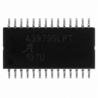
A3979SLPTR-T Allegro Microsystems Inc, A3979SLPTR-T Datasheet - Page 8

A3979SLPTR-T
Manufacturer Part Number
A3979SLPTR-T
Description
IC DRIVER MICROSTEPPING 28-TSSOP
Manufacturer
Allegro Microsystems Inc
Datasheet
1.A3979SLPTR-T.pdf
(14 pages)
Specifications of A3979SLPTR-T
Applications
Stepper Motor Driver
Number Of Outputs
1
Current - Output
±2.5A
Voltage - Load
8 V ~ 35 V
Voltage - Supply
3 V ~ 5.5 V
Operating Temperature
-20°C ~ 85°C
Mounting Type
Surface Mount
Package / Case
28-TSSOP Exposed Pad, 28-eTSSOP, 28-HTSSOP
Motor Type
DMOS
No. Of Outputs
2
Output Current
2.5A
Output Voltage
35V
Supply Voltage Range
3V To 5.5V
Driver Case Style
TSSOP
No. Of Pins
28
Operating Temperature Range
-20°C To +85°C
Operating Current
8mA
Operating Temperature Classification
Commercial
Package Type
TSSOP EP
Operating Supply Voltage (min)
3V
Operating Supply Voltage (typ)
5V
Operating Supply Voltage (max)
5.5V
Lead Free Status / RoHS Status
Lead free / RoHS Compliant
Lead Free Status / RoHS Status
Lead free / RoHS Compliant, Lead free / RoHS Compliant
Other names
620-1148-2
A3979SLPTR-T
A3979SLPTR-T
Available stocks
Company
Part Number
Manufacturer
Quantity
Price
Part Number:
A3979SLPTR-T
Manufacturer:
ALLEGRO/雅丽高
Quantity:
20 000
A3979
Fixed Off-Time.
cuitry uses a one-shot timer to control the duration of time
that the MOSFETs remain off. The one shot off-time, t
is determined by the selection of external resistors, R
capacitors, C
ground. The off-time, over a range of values of C
to 1500 pF and R
RC Blanking.
PWM control circuit, the CTx component sets the compara-
tor blanking time. This function blanks the output of the
current-sense comparators when the outputs are switched
by the internal current-control circuitry. The comparator
outputs are blanked to prevent false overcurrent detection
due to reverse recovery currents of the clamp diodes, or to
switching transients related to the capacitance of the load.
The blank time t
Charge Pump
used to generate a gate supply greater than that of VBB for
driving the source-side DMOS gates. A 0.22 μF ceramic
capacitor should be connected between CP1 and CP2 for
pumping purposes. In addition, a 0.22 μF ceramic capacitor
is required between VCP and VBB, to act as a reservoir for
operating the high-side DMOS gates.
V
operate the sink-side DMOS outputs. The VREG pin must
be decoupled with a 0.22 μF capacitor to ground. V
internally monitored, and in the case of a fault condition, the
DMOS outputs of the device are disabled.
Enable Input
enables all of the DMOS outputs. When set to a logic high,
the outputs are disabled. The inputs to the translator (STEP,
DIR, MS1, and MS2), all remain active, independent of the
¯ E ¯ ¯ N ¯ ¯ A ¯ ¯ B ¯ ¯ L ¯ ¯ E ¯ input state.
Shutdown.
fault, such as overtemperature (excess T
REG
(VREG)
Tx
During normal operation, in the event of a
, connected from each R
.
BLANK
T
This internally-generated voltage is used to
(
In addition to the fixed off-time of the
¯ E ¯ ¯ N ¯ ¯ A ¯ ¯ B ¯ ¯ L ¯ ¯ E ¯
(CP1 and CP2). The charge pump is
= 12 kΩ to 100 kΩ is approximated by:
t
The internal PWM current-control cir-
BLANK
can be approximated by:
t
OFF
= 1400C
= R
)
.
This active-low input
T
C
T
T
DMOS Microstepping Driver with Translator
Cx
J
) or an undervolt-
timing terminal to
T
= 470 pF
REG
Tx
OFF
, and
is
,
age on VCP, the outputs of the device are disabled until the
fault condition is removed.
At power up, and in the event of low V
lockout (UVLO) circuit disables the drivers and resets the
translator to the Home state.
Sleep Mode
is used to minimize power consumption when the motor is
not in use. It disables much of the internal circuitry includ-
ing the output DMOS FETs, current regulator, and charge
pump. Setting this to a logic high allows normal operation,
as well as start-up (at which time the A3979 drives the
motor to the Home microstep position). When bringing the
device out of Sleep mode, in order to allow the charge pump
(gate drive) to stabilize, provide a delay of 1 ms before issu-
ing a step command signal on the STEP input.
Percent Fast Decay Input (PFD). When a STEP
input signal commands a lower output current than the
previous step, it switches the output current decay to either
Slow, Fast, or Mixed decay mode, depending on the voltage
level at the PFD input. If the voltage at the PFD input is
greater than 0.6 × V
If the voltage on the PFD input is less than 0.21 × V
Fast decay mode is selected. Mixed decay mode is selected
when V
the next section. This terminal should be decoupled with a
0.1 μF capacitor.
Mixed Decay Operation. If the voltage on the PFD input
is between 0.6 × V
in Mixed decay mode, as determined by the step sequence
(shown in figures 2 through 5). As the trip point is reached,
the device goes into Fast decay mode until the voltage
on the RCx terminal decays to the same level as voltage
applied to the PFD terminal. The time that the device oper-
ates in fast decay is approximated by:
After this Fast decay portion, the device switches to Slow
decay mode for the remainder of the fixed off-time period.
PFD
is between these two levels, as described in
t
FD
(
¯ S ¯ ¯ L ¯ ¯ E ¯ ¯ E ¯ ¯ P ¯
= R
DD
DD
, then Slow decay mode is selected.
and 0.21 × V
T
C
T
115 Northeast Cutoff, Box 15036
Allegro MicroSystems, Inc.
Worcester, Massachusetts 01615-0036 (508) 853-5000
www.allegromicro.com
ln (0.6V
). This active-low control input
DD
DD
, the bridge operates
DD
/V
, the undervoltage
PFD
)
DD
, then
8


