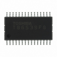
TB6539FG(EL) Toshiba, TB6539FG(EL) Datasheet

TB6539FG(EL)
Specifications of TB6539FG(EL)
Related parts for TB6539FG(EL)
TB6539FG(EL) Summary of contents
Page 1
... TOSHIBA Bi-CMOS Integrated Circuit Silicon Monolithic TB6539N/NG, TB6539F/FG 3-PHASE FULL-WAVE SINE-WAVE PWM BRUSHLESS MOTOR CONTROL Features • Sine-wave PWM control • Built-in triangular-wave generator (carrier cycle = f /252 (Hz)) osc • Built-in lead angle control function (0 to 58° steps) • Built-in dead time function • ...
Page 2
Block Diagram X in 14/17 System clock generator X 15/19 out HU 21/26 Position detector HV 20/25 HW 19/23 V 22/27 e Regulator V 1/1 CC P-GND 3/4 S-GND 13/16 V 24/30 refout Power-on reset RES 18/22 I 2/3 dc ...
Page 3
Pin Description Pin No. Symbol TB6539N TB6539F /NG /FG Positional signal input pin U Positional signal input pin V Positional signal input pin W Rotation direction 17 21 CW/CCW signal input ...
Page 4
Input/Output Equivalent Circuits Pin Description Symbol Positional signal input pin U HU Positional signal input pin V HV Positional signal input pin W HW Forward/reverse switching input pin CW/CCW L: Forward (CW) H: Reverse (CCW) Reset input RES L: Stops ...
Page 5
Pin Description Symbol Output logic select signal input pin OS L: Active low H: Active high Over-current protection I dc signal input pin Clock signal input pin X in Clock signal output pin X out Reference voltage signal Vrefout output ...
Page 6
Pin Description Symbol FG signal output pin FG Turn-on signal output pin U U Turn-on signal output pin V V Turn-on signal output pin W W Turn-on signal output pin X X Turn-on signal output pin Y Y Turn-on signal ...
Page 7
Absolute Maximum Ratings Characteristics Supply voltage Input voltage Turn-on signal output current N/NG Type Power dissipation F/ FG Type Operating temperature Storage temperature Note 1: V pin LA, REV (1) e Note 2: V pin: HU, ...
Page 8
V Electrical Characteristics Characteristics Symbol Circuit I CC Supply current ( (2) Input current ( (2) High Input voltage V in Low Input hysteresis ...
Page 9
Functional Description Basic operation On start-up, the motor is driven by the square-wave turn-on signal based on a positional signal. When the positional signal reaches number of rotations higher, the rotor position is inferred from ...
Page 10
Protecting input pin 1. Over-current protection (Pin When the DC-link-current exceeds the internal reference voltage, gate block protection is performed. Over-current protection is released for each carrier frequency. Reference voltage = 0.5 V (typ.) 2. Gate block ...
Page 11
Operation Flow Positional signal Position (Hall IC) detector Voltage instruction System clock Oscillator generator (Note) 92% 100% Phase U Counter Phase V Phase matching (Phase U) Phase Sine-wave pattern W (modulation signal) Triangular wave (carrier frequency) Driven by square wave ...
Page 12
The modulation waveform is generated using Hall signals. The modulation waveform is then compared with the triangular wave and a sine-wave PWM signal is generated. The time (electrical angle: 60°) from the rising (or falling) edges of the three Hall ...
Page 13
Timing Charts H u Hall signal H v (input signal FG (output Turn-on signal W when driven by square wave X (output Modulation waveform when driven by sine wave (inside of ...
Page 14
Operating Waveform When Driven by Square Wave Hall signal Output waveform stabilize the bootstrap voltage, the lower outputs (X, Y, and Z) are always turned ...
Page 15
Operating Waveform When Driven by Sine-Wave PWM Generation inside of IC Phase U Phase V Phase W Output waveform Inter-line voltage V UV (U- (V- (W-U) When driven by a ...
Page 16
Example of Application Circuit 14/17 X System clock in 15/19 X out 21/26 HU 20/25 HV 19/23 HW 22/ 1/1 Regulator V CC 3/4 (Note 2) P-GND 13/16 S-GND 24/30 V refout Power-on reset 18/22 RES 2/3 MCU ...
Page 17
Package Dimensions Weight: 1.62 g (typ.) TB6539N/NG/F/FG 17 2007-07-17 ...
Page 18
Package Dimensions Weight: 0.63 g (typ.) TB6539N/NG/F/FG 18 2007-07-17 ...
Page 19
... Application Circuits The application circuits shown in this document are provided for reference purposes only. Thorough evaluation is required, especially at the mass production design stage. Toshiba does not grant any license to any industrial property rights by providing these examples of application circuits. 5. Test Circuits Components in the test circuits are used only to obtain and confirm the device characteristics. These components and circuits are not guaranteed to prevent malfunction or failure from occurring in the application equipment ...
Page 20
... The information contained herein is presented only as a guide for the applications of our products. No responsibility is assumed by TOSHIBA for any infringements of patents or other rights of the third parties which may result from its use. No license is granted by implication or otherwise under any patents or other rights of TOSHIBA or the third parties ...


