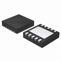
LTC4413EDD#PBF Linear Technology, LTC4413EDD#PBF Datasheet - Page 6

LTC4413EDD#PBF
Manufacturer Part Number
LTC4413EDD#PBF
Description
IC IDEAL DIODE DUAL 10-DFN
Manufacturer
Linear Technology
Datasheet
1.LTC4413EDDPBF.pdf
(12 pages)
Specifications of LTC4413EDD#PBF
Applications
Handheld/Mobile Devices
Fet Type
P-Channel
Number Of Outputs
2
Internal Switch(s)
Yes
Delay Time - On
11µs
Delay Time - Off
2µs
Voltage - Supply
2.5 V ~ 5.5 V
Current - Supply
25µA
Operating Temperature
-40°C ~ 85°C
Mounting Type
Surface Mount
Package / Case
10-DFN
Input Voltage
5.5V
No. Of Outputs
2
Power Dissipation Pd
1.5W
Supply Voltage Range
2.5V To 5.5V
No. Of Pins
10
Operating Temperature Range
-40°C To +85°C
Msl
MSL 1 - Unlimited
Termination Type
SMD
Rohs Compliant
Yes
Filter Terminals
SMD
Lead Free Status / RoHS Status
Lead free / RoHS Compliant
Available stocks
Company
Part Number
Manufacturer
Quantity
Price
TYPICAL PERFORMANCE CHARACTERISTICS
LTC4413
PIN FUNCTIONS
INA (Pin 1): Primary Ideal Diode Anode and Positive
Power Supply. Bypass INA with a ceramic capacitor of at
least 1μF. 1Ω snub resistors in series with a capacitor and
higher valued capacitances are recommended when large
inductances are in series with this input. Limit slew rate
on this pin to less than 0.5V/μs. This pin can be grounded
when not used.
ENBA (Pin 2): Enable Low for Diode A. Weak (3μA) pull-
down. Pull this pin high to shut down this power path.
Tie to GND to enable. Refer to Table 1 for mode control
functionality. This pin can be left fl oating, weak pull-down
internal to the LTC4413.
GND (Pins 3, 11): Power and Signal Ground for the IC. The
exposed pad of the package, Pin 11, must be soldered to
PCB ground to provide both electrical contact to ground
and good thermal contact to the PCB.
ENBB (Pin 4): Enable Low for Diode B. Weak (3μA) pull-
down. Pull this pin high to shut down this power path.
Tie to GND to enable. Refer to Table 1 for mode control
functionality. This pin can be left fl oating, weak pull-down
internal to the LTC4413.
INB (Pin 5): Secondary Ideal Diode Anode and Positive
Power Supply. Bypass INB with a ceramic capacitor of at
least 1μF. 1Ω snub resistors in series with a capacitor and
6
100E-9
10E-6
10E-9
1E-6
1E-9
0
– I
LEAK
80°C
40°C
0°C
–40°C
1
vs V
REVERSE
2
V
REVERSE
3
(V)
4
4413 G16
5
1.00
0.98
0.96
0.94
0.92
0.90
1.0E-3
Effi ciency vs Load Current
10.0E-3
LOAD CURRENT (A)
100.0E-3
higher valued capacitances are recommended when large
inductances are in series with this input. Limit slew rate
on this pin to less than 0.5V/μs. This pin can be grounded
when not used.
OUTB (Pin 6): Secondary Ideal Diode Cathode and Output.
Bypass OUTB with a high (1mΩ min) ESR ceramic capacitor
of at least 4.7μF. Limit slew rate on this pin to less than
0.5V/μs. This pin must be left fl oating when not in use.
NC (Pin 7): No Internal Connection.
NC (Pin 8): No Internal Connection.
STAT (Pin 9): Status Condition Indicator. Weak (9μA)
pull-down current output. When terminated, STAT = high
indicates diode conducting.
The function of the STAT pin depends on the mode that
has been selected. Table 2 describes the STAT pin output
current as a function of the mode selected as well as the
conduction state of the two diodes. This pin can also be
left fl oating or grounded.
OUTA (Pin 10): Primary Ideal Diode Cathode and Output.
Bypass OUTA with a high (1mΩ min) ESR ceramic capacitor
of at least 4.7μF. Limit slew rate on this pin to less than
0.5V/μs. This pin must be left fl oating when not in use.
1.0E+0
1351 G13
10.0E+0
600
500
400
300
200
100
0
1
Power Loss LTC4413 vs 1N5817
1N5817
500
1000
I
LOAD
(mA)
1500
LTC4413
2000
4413 G19
4413fc
2500


