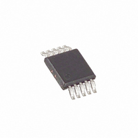
MAX8555AEUB+ Maxim Integrated Products, MAX8555AEUB+ Datasheet - Page 8

MAX8555AEUB+
Manufacturer Part Number
MAX8555AEUB+
Description
IC CNTRLR MOSFET ORING 10-UMAX
Manufacturer
Maxim Integrated Products
Datasheet
1.MAX8555AEUB.pdf
(17 pages)
Specifications of MAX8555AEUB+
Applications
Telecom Supplies, Rectifiers
Fet Type
N-Channel
Number Of Outputs
1
Internal Switch(s)
No
Delay Time - Off
100ns
Voltage - Supply
8 V ~ 13.25 V
Current - Supply
2mA
Operating Temperature
-40°C ~ 85°C
Mounting Type
Surface Mount
Package / Case
10-MSOP, Micro10™, 10-uMAX, 10-uSOP
Lead Free Status / RoHS Status
Lead free / RoHS Compliant
Delay Time - On
-
Lead Free Status / Rohs Status
Lead free / RoHS Compliant
Low-Cost, High-Reliability, 0.5V to 3.3V ORing
MOSFET Controllers
8
PIN
10
_______________________________________________________________________________________
1
2
3
4
5
6
7
8
9
FAULT
NAME
TIMER
GATE
GND
UVP
OVP
CS+
V
CS-
VL
DD
FUNCTION
Gate-Drive Output. Nominal GATE load is a 0.01µF capacitor to ground. Gate is discharged to GND in
shutdown.
Ground
Low-Voltage Optional Input Power. Leave disconnected when V
when V
Power-Supply Input. Connect to an 8V to 13.25V supply or connect to VL when using a 3V to 5.5V supply.
Bypass V
Undervoltage-Protection Input. Connect UVP to the center of a resistor-divider from CS+ to GND. Connect
UVP to VL to disable the undervoltage protection.
Timer Input. Connect a resistor from TIMER to GND to select the charge-pump operating frequency. Drive
TIMER low (< 0.5V) to disable the gate drive. Drive TIMER high (above 1.5V) for charge-pump operation
at 550kHz.
Open-Drain Fault Output. FAULT is high impedance during normal operation and is pulled to GND when a
fault condition occurs. Connect a pullup resistor of 10k or higher value (50k typ) to a voltage rail of 5.5V
or lower.
Overvoltage-Protection Input. Connect OVP to the center of a resistor-divider from the output bus to GND.
Connect OVP to GND to disable the overvoltage protection.
Current-Sensing Input. Connect CS- to the positive side of the system bus. Bypass with a 1000pF capacitor
to GND.
Current-Sensing Input. Connect CS+ to the positive side of the input power. Bypass with a 1000pF capacitor
to GND.
DD
DD
= 3V to 5.5V. Bypass VL to GND with a 0.01µF capacitor.
with a 0.01µF capacitor to ground.
DD
= 8V to 13.25V, or connect V
Pin Description
DD
to VL


