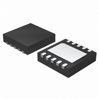
LTC4413EDD-1#PBF Linear Technology, LTC4413EDD-1#PBF Datasheet - Page 9

LTC4413EDD-1#PBF
Manufacturer Part Number
LTC4413EDD-1#PBF
Description
IC IDEAL DIODE DUAL 10-DFN
Manufacturer
Linear Technology
Datasheet
1.LTC4413EDD-1PBF.pdf
(16 pages)
Specifications of LTC4413EDD-1#PBF
Applications
Handheld/Mobile Devices
Fet Type
P-Channel
Number Of Outputs
2
Internal Switch(s)
Yes
Delay Time - On
11µs
Delay Time - Off
2µs
Voltage - Supply
2.5 V ~ 5.5 V
Current - Supply
40µA
Operating Temperature
-40°C ~ 85°C
Mounting Type
Surface Mount
Package / Case
10-DFN
Lead Free Status / RoHS Status
Lead free / RoHS Compliant
Available stocks
Company
Part Number
Manufacturer
Quantity
Price
OPERATION
The LTC4413-1/LTC4413-2 are described with the aid of the
Block Diagram. Operation begins when the power source at
V
voltage of 2.4V and the corresponding control pin ENBA or
ENBB is low. If only the voltage at the V
the internal power source (V
pin. The amplifi er (A) pulls a current proportional to the
difference between V
of the internal PFET (PA), driving this gate voltage below
V
voltage drop (V
regulates V
drop. The system is now in forward regulation and the
load at V
load current varies, V
until the load current exceeds the transistor’s (PA) ability
to deliver the current as V
point, the PFET behaves as a fi xed resistor, R
the forward voltage increases slightly with increased load
current. As the magnitude of I
that I
current to the constant value I
The characteristics for parameters R
I
LTC4413-1/LTC4413-2 forward voltage drop versus that
of a Schottky.
If another supply is provided at V
LTC4413-2 likewise regulate the gate voltage on PB to
OC
INA
INA
are specifi ed with the aid of Figure 1, illustrating the
. This turns on PA. As V
or V
LOAD
INB
OUTA
> I
GATEA
rises above the undervoltage lockout (UVLO)
OC
is powered from the supply at V
) the LTC4413-1/LTC4413-2 fi xes the load
FWD
to maintain the small forward voltage
) of 15mV below V
INA
GATEA
and V
GATEA
is controlled to maintain V
DD
OUTA
OUT
OUTA
) is supplied from the V
OC
approaches GND. At this
increases further, (such
from the gate (V
to protect the device.
pulls up to a forward
INB
FWD
INA
, the LTC4413-1/
INA
, R
I
FWD
I
OC
, the LTC4413
pin is present,
0
Figure 1. The LTC4413 vs the 1N5817
ON
ON
0
LTC4413-1
LTC4413-2
, V
INA
V
, whereby
FWD
FWD
. As the
GATEA
FORWARD VOLTAGE (V)
SLOPE: 1/R
FWD
and
INA
)
SLOPE: 1/R
FWD
maintain the output voltage, V
voltage V
voltage at V
input voltage as the internal supply (V
ideal diode operates independently of the fi rst ideal diode
function.
When an alternate power source is connected to the load
at V
increased voltage at V
voltage V
V
to V
LTC4413-1/LTC4413-2 (V
from the V
V
Power to the load is being delivered from an alternate
supply, and only a small current (I
sourced to V
When the selected channel of the LTC4413-1/LTC4413-2
is in reverse turn-off mode or both channels are disabled,
the STAT pin sinks 11μA of current (I
Channel selection is accomplished using the two ENB
pins, ENBA and ENBB. When the ENBA input is asserted
(high), PA has its gate voltage pulled to V
PA. A 3.5μA pull-down current on the ENB pins ensures
a low level at these inputs if left fl oating.
OUTA
OUTB
ON
OUTA
DD
1N5817
). The system is now in the reverse turn-off mode.
is higher than V
, turning off PA. The internal power source for the
(or V
INB
GATEA
441312 F01
OUTA
LTC4413-1/LTC4413-2
. If this alternate supply, V
INA
INA
OUTB
, reducing the current through PA. When
, the LTC4413-1/LTC4413-2 selects this
pin, only if V
to sense the potential at V
), the LTC4413-1/LTC4413-2 sense the
OUTA
INA
+ V
DD
, and amplifi er A increases the
) then diverts to draw current
RTO
OUTA
OUTB
, V
LEAK
is larger than V
GATEA
, just below the input
SON
) is drawn from or
DD
INB
will be pulled up
) if connected.
). This second
DD
INA
, exceeds the
, turning off
.
INB
441312fd
9
(or


