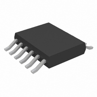
LTC3127EMSE#PBF Linear Technology, LTC3127EMSE#PBF Datasheet - Page 7

LTC3127EMSE#PBF
Manufacturer Part Number
LTC3127EMSE#PBF
Description
IC BUCK BOOST SYNC ADJ 12MSOP
Manufacturer
Linear Technology
Datasheet
1.LTC3127EDDPBF.pdf
(20 pages)
Specifications of LTC3127EMSE#PBF
Applications
Energy Harvesting
Current - Supply
400µA
Voltage - Supply
1.8 V ~ 5.5 V
Operating Temperature
-40°C ~ 85°C
Mounting Type
Surface Mount
Package / Case
12-MSOP Exposed Pad
Primary Input Voltage
3.6V
No. Of Outputs
1
Output Voltage
5.25V
Output Current
1A
No. Of Pins
12
Operating Temperature Range
-40°C To +85°C
Msl
MSL 1 - Unlimited
Rohs Compliant
Yes
Lead Free Status / RoHS Status
Lead free / RoHS Compliant
Available stocks
Company
Part Number
Manufacturer
Quantity
Price
pin FuncTions
SW1 (Pin 1): Switch Pin Where Internal Switches A and
B Are Connected. Connect inductor from SW1 to SW2.
Minimize trace length to reduce EMI.
V
10μF or greater ceramic capacitor should be placed as
close to V
SHDN (Pin 3): Logic-Controlled Shutdown Input.
MODE (Pin 4): Pulse Width Modulation/Burst Mode
Selection Input.
PROG (Pin 5): Sets the Average Input Current Limit
Threshold. Connect a resistor from PROG to ground. See
below for component value selection.
IN
SHDN = High: Normal Operation
SHDN = Low: Shutdown
MODE = High: Burst Mode Operation
MODE = Low: PWM Operation Only. Forced continuous
conduction mode.
R
(Pin 2): Input Supply Pin. Internal V
PROG
= 54.92 • I
IN
and PGND as possible.
LIMIT
(A) + 4.94 (kΩ)
(DD Package)
CC
for the IC. A
SGND (Pin 6): Signal Ground for the IC. Terminate the
PROG resistor, compensation components and the output
voltage divider to SGND.
FB (Pin 7): Feedback Pin. Connect resistor divider tap here.
The output voltage can be adjusted from 1.8V to 5.25V.
The feedback reference voltage is 1.195V.
V
components from this pin to SGND.
V
the output filter capacitor from this pin to GND. A minimum
value of 22µF is recommended. Output capacitors must
be low ESR.
SW2 (Pin 10): Switch Pin Where Internal Switches C and
D Are Connected. Minimize trace length to reduce EMI.
PGND (Exposed Pad Pin 11): Power Ground. The exposed
pad must be soldered to the PCB ground plane.
C
OUT
V
(Pin 8): Error Amplifier Output. Place compensation
OUT
(Pin 9): Output of the Synchronous Rectifier. Connect
=
1 195
.
•
1
+
R
R
2
1
V
LTC3127
3127f


