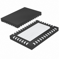
LTC3586EUFE#PBF Linear Technology, LTC3586EUFE#PBF Datasheet - Page 11

LTC3586EUFE#PBF
Manufacturer Part Number
LTC3586EUFE#PBF
Description
IC MANAGER USB PWR HI-EFF 38QFN
Manufacturer
Linear Technology
Datasheet
1.LTC3586EUFEPBF.pdf
(36 pages)
Specifications of LTC3586EUFE#PBF
Applications
Handheld/Mobile Devices
Voltage - Supply
4.35 V ~ 5.5 V
Operating Temperature
-40°C ~ 85°C
Mounting Type
Surface Mount
Package / Case
38-QFN
Lead Free Status / RoHS Status
Lead free / RoHS Compliant
Current - Supply
-
Available stocks
Company
Part Number
Manufacturer
Quantity
Price
pin FuncTions
I
control the current limit of the PowerPath switching
regulator. See Table 1.
Table 1. USB Current Limit Settings
LDO3V3 (Pin 3): 3.3V LDO Output Pin. This pin provides
a regulated always-on 3.3V supply voltage. LDO3V3
gets its power from V
such as a watch dog microprocessor or real time clock.
A 1µF capacitor is required from LDO3V3 to ground. If
the LDO3V3 output is not used it should be disabled by
connecting it to V
CLPROG (Pin 4): USB Current Limit Program and Moni-
tor Pin. A resistor from CLPROG to ground determines
the upper limit of the current drawn from the V
A fraction of the V
when the synchronous switch of the PowerPath switching
regulator is on. The switching regulator delivers power until
the CLPROG pin reaches 1.188V. Several V
settings are available via user input which will typically
correspond to the 500mA and 100mA USB specifications.
A multilayer ceramic averaging capacitor is required at
CLPROG for filtering.
NTC (Pin 5): Input to the Thermistor Monitoring Circuits.
The NTC pin connects to a battery’s thermistor to deter-
mine if the battery is too hot or too cold to charge. If the
battery’s temperature is out of range, charging is paused
until it re-enters the valid range. A low drift bias resistor
is required from V
from NTC to ground. If the NTC function is not desired,
the NTC pin should be grounded.
V
Regulator 4. A 10µF MLCC capacitor should be placed as
close to the pins as possible.
LIM0
OUT4
, I
(I
(Pins 6, 7): Power Output for the (Boost) Switching
LIM1
LIM1
0
0
1
1
)
(Pins 1, 2): Logic Inputs. I
OUT
BUS
BUS
.
(I
OUT
to NTC and a thermistor is required
current is sent to the CLPROG pin
LIM0
0
1
0
1
. It may be used for light loads
)
USB SETTING
1x Mode (USB 100mA Limit)
10x Mode (Wall 1A Limit)
Suspend
5x Mode (USB 500mA Limit)
BUS
LIM0
current limit
and I
BUS
LIM1
pin.
SW4 (Pin 8): Switch Node for the (Boost) Switching
Regulator 4. An external inductor connects between this
pin and V
MODE (Pin 9): Digital Input. The MODE pin controls dif-
ferent modes of operation for the switching regulators
according to Table 2.
Table 2. Switching Regulators Mode
FB4 (Pin 10): Feedback Input for the (Boost) Switching
Regulator 4. When the control loop is complete, the volt-
age on this pin servos to 0.8V.
FB3 (Pin 11): Feedback Input for (Buck-Boost) Switching
Regulator 3. When regulator 3’s control loop is complete,
this pin servos to 0.8V.
V
pensation Node for (Buck-Boost) Switching Regulator 3.
External Type I or Type III compensation (to FB3) connects
to this pin. See the Applications Information section for
selecting buck-boost compensation components.
SWAB3 (Pin 13): Switch Node for (Buck-Boost) Switch-
ing Regulator 3. Connected to Internal Power Switches A
and B. An external inductor connects between this node
and SWCD3.
V
Regulator 3. These pins will generally be connected to V
A 1µF MLCC capacitor is recommended on these pins.
V
Switching Regulator 3.
EN3 (Pin 18): Digital Input. This input enables the
buck-boost switching regulator 3.
SWCD3 (Pin 19): Switch Node for (Buck-Boost) Switch-
ing Regulator 3 Connected to Internal Power Switches C
and D. An external inductor connects between this node
and SWAB3.
C3
IN3
OUT3
(Pin 12): Output of the Error Amplifier and Voltage Com-
(Pins 14, 15): Power Input for (Buck-Boost) Switching
Mode
0
1
(Pins 16, 17): Output Voltage for (Buck-Boost)
IN4
.
LTC3586/LTC3586-1
Pulse-Skip
Burst
Buck
REGULATION MODE
Buck-Boost
PWM
Burst
Pulse-Skip
Pulse-Skip
Boost
OUT
3586fb
.


